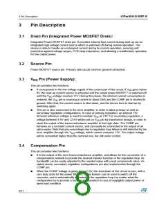
5 Operation Description
VIPer50A-E/ASP-E
As soon as the power goes below this limit, the auxiliary secondary voltage starts to increase
above the 13V regulation level, forcing the output voltage of the transconductance amplifier to
low state (V
< V
). This situation leads to the shutdown mode where the power
COMP
COMPth
switch is maintained in the Off state, resulting in missing cycles and zero duty cycle. As soon as
gets back to the regulation level and the V threshold is reached, the device
V
DD
COMPth
operates again. The above cycle repeats indefinitely, providing a burst mode of which the
effective duty cycle is much lower than the minimum one when in normal operation. The
equivalent switching frequency is also lower than the normal one, leading to a reduced
consumption on the input main supply lines. This mode of operation allows the VIPer50A-E/
ASP-E to meet the new German "Blue Angel" Norm with less than 1W total power consumption
for the system when working in stand-by mode. The output voltage remains regulated around
the normal level, with a low frequency ripple corresponding to the burst mode. The amplitude of
this ripple is low, because of the output capacitors and low output current drawn in such
conditions.The normal operation resumes automatically when the power gets back to higher
levels than P
.
STBY
5.3
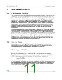
High Voltage Start-up Current Source
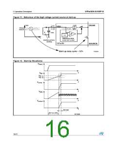
An integrated high voltage current source provides a bias current from the DRAIN pin during
the start-up phase. This current is partially absorbed by internal control circuits which are
placed into a standby mode with reduced consumption and also provided to the external
capacitor connected to the V pin. As soon as the voltage on this pin reaches the high voltage
DD
threshold V
of the UVLO logic, the device becomes active mode and starts switching. The
DDon
start-up current generator is switched off, and the converter should normally provide the
needed current on the V pin through the auxiliary winding of the transformer, as shown on
DD
(see Figure 11).
In case there are abnormal conditions where the auxiliary winding is unable to provide the low
voltage supply current to the V pin (i.e. short circuit on the output of the converter), the
DD
external capacitor discharges to the low threshold voltage V
of the UVLO logic, and the
DDoff
device goes back to the inactive state where the internal circuits are in standby mode and the
start-up current source is activated. The converter enters a endless start-up cycle, with a start-
up duty cycle defined by the ratio of charging current towards discharging when the device tries
to start. This ratio is fixed by design to 2A to 15A, which gives a 12% start-up duty cycle while
the power dissipation at start-up is approximately 0.6W, for a 230Vrms input voltage.
This low value start-up duty cycle prevents the application of stress to the output rectifiers as
well as the transformer when a short circuit occurs.
The external capacitor C
on the V pin must be sized according to the time needed by the
DD
VDD
converter to start up, when the device starts switching. This time t depends on many
SS
parameters, among which transformer design, output capacitors, soft start feature, and
compensation network implemented on the COMP pin. The following formula can be used for
defining the minimum capacitor needed:
IDDtSS
where: CVDD > --------------------
VDDhyst
I
is the consumption current on the V pin when switching. Refer to specified I
and I
2
DD
DD
DD
DD1
values.
t
is the start up time of the converter when the device begins to switch. Worst case is
SS
generally at full load.
12/31

 STMICROELECTRONICS [ ST ]