VIPer20/SP/DIP - VIPer20A/ASP/ADIP
ELECTRICAL CHARACTERISTICS (continued)
OSCILLATOR SECTION
Symbol
Parameter
Test Conditions
Min
Typ
Max
Unit
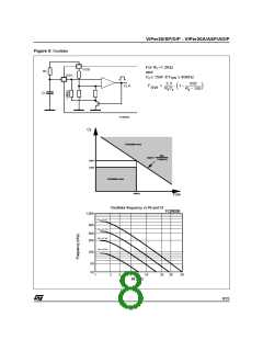
R =8.2KΩ; C =2.4nF
t
t
90
100
110
kHz
Oscillator Frequency
Total Variation
V
=9 to 15V;
DD
F
SW
with R ± 1%; C ± 5%
t
t
(see fig. 6 and fig. 9)
V
Oscillator Peak Voltage
Oscillator Valley Voltage
7.1
3.7
V
V
OSCih
V
OSCil
ERROR AMPLIFIER SECTION
Symbol
Parameter
Test Conditions
I =0mA
COMP
Min
Typ
13
Max
Unit
V
V
V
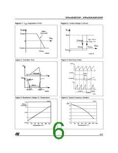
Regulation Point
(see fig. 1) 12.6
13.4
DDreg
DD
∆V
Total Variation
T =0 to 100°C
2
%
DDreg
j
150
kHz
From Input =V to Output = V
DD
COMP
G
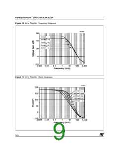
Unity Gain Bandwidth
BW
COMP pin is open
(see fig. 10)
(see fig. 10)
(see fig. 1)
A
Open Loop Voltage Gain COMP pin is open
45
52
1.5
0.2
4.5
dB
mA/V
V
VOL
G
DC Transconductance
Output Low Level
V
=2.5V
1.1
1.9
m
COMP
V
I
I
= -400µA; V =14V
DD
COMPLO
COMP
COMP
V
Output High Level
=400µA; V =12V
V
COMPHI
DD
Output Low Current
Capability
I
V
=2.5V; V =14V
-600
600
µA
µA
COMPLO
COMP
COMP
DD
Output High Current
Capability
I
V
=2.5V; V =12V
DD
COMPHI
PWM COMPARATOR SECTION
Symbol
Parameter
/ ∆I
Test Conditions
Min
Typ
6
Max
Unit
V/A
V
H
∆V
V
=1 to 3 V
4.2
7.8
ID
COMP
DPEAK
COMP
V
V
Offset
I
=10mA
0.5
0.67
COMPoff
COMP
DPEAK
I
Peak Current Limitation
V
=12V; COMP pin open
0.5
0.9
A
Dpeak
DD
Current Sense Delay to
Turn-Off
t
t
I =1A
250
ns
d
D
Blanking Time
250
350
360
ns
ns
b
t
Minimum On Time
on(min)
SHUTDOWN AND OVERTEMPERATURE SECTION
Symbol
Parameter
Restart Threshold
Disable Set Up Time
Test Conditions
Min
Typ
0.5
1.7
Max
Unit
V
V
(see fig. 4)
(see fig. 4)
COMPth
t
5
µs
DISsu
Thermal Shutdown
Temperature
T
(See fig. 8)
(See fig. 8)
140
170
40
190
°C
°C
tsd
Thermal Shutdown
Hysteresis
T
hyst
5/25

 STMICROELECTRONICS [ ST ]