TN25 and TYNx25 Series
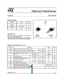
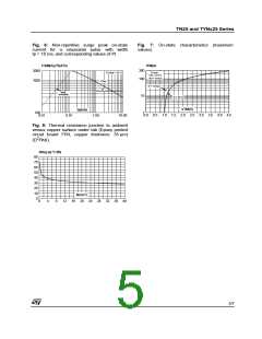
Fig. 1: Maximum average power dissipation
Fig. 2-1: Average and D.C. on-state current
versus average on-state current.
versus case temperature.
IT(av)(A)
P(W)
28
24
22
D.C.
26
α = 180°
24
22
20
20
18
16
14
12
10
8
6
4
2
0
18
16
14
12
10
8
α = 180°
360°
6
4
IT(av)(A)
10
α
Tcase(°C)
50 75
2
0
0
2
4
6
8
12
14
16
0
25
100
125
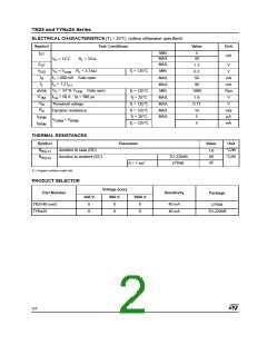
Fig. 2-2: Average and D.C. on-state current
versus ambient temperature (copper surface
under tab: S = 1 cm² (for D²PAK).
Fig. 3: Relative variation of thermal impedance
versus pulse duration.
IT(av)(A)
K = [Zth/Rth]
4.0
3.5
1.00
Zth(j-c)
D.C.
3.0
2.5
α = 180°
0.10
0.01
Zth(j-a)
2.0
1.5
1.0
0.5
tp(s)
Tamb(°C)
0.0
1E-3
1E-2
1E-1
1E+0
1E+1
1E+2 5E+2
0
25
50
75
100
125
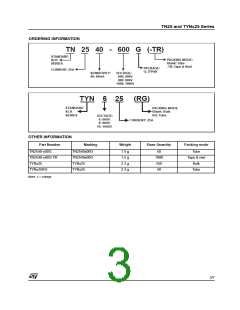
Fig. 4: Relative variation of gate trigger current,
holding current and latching current versus
junction temperature.
Fig. 5: Surge peak on-state current versus
number of cycles.
IGT,IH,IL [Tj] / IGT,IH,IL [Tj = 25 °C]
ITSM(A)
2.5
350
300
2.0
tp = 10ms
IGT
250
One cycle
Non repetitive
Tj initial = 25°C
1.5
200
150
100
50
IH & IL
1.0
Repetitive
Tcase = 100 °C
0.5
Tj(°C)
Number of c
ycles
100
0.0
0
-40 -20
0
20
40
60
80 100 120 140
1
10
1000
4/7

 STMICROELECTRONICS [ ST ]