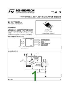
TDA8172
ABSOLUTE MAXIMUM RATINGS
Symbol
Parameter
Value
35
Unit
V
VS
Supply Voltage (pin 2)
Flyback Peak Voltage
Voltage at Pin 3
V5, V6
V3
60
V
+ Vs
V1, V7
Amplifier Input Voltage
+ Vs
– 0.5
V
Io
Output Peak Current (non repetitive, t = 2 ms)
Output Peak Current at f = 50 or 60 Hz, t ≤ 10 µs
Output Peak Current at f = 50 or 60 Hz, t > 10 µs
Pin 3 DC Current at V5 < V2
2.5
A
A
Io
Io
3
2
A
I3
100
mA
A
I3
Pin 3 Peak to Peak Flyback Current at f = 50 or 60 Hz, tfly ≤ 1.5 ms
Total Power Dissipation at Tcase = 90 °C
3
20
Ptot
Tstg, Tj
W
°C
Storage and Junction Temperature
– 40, +150
THERMAL DATA
Symbol
Parameter
Thermal Resistance Junction-case
Value
Unit
Rth (j–c)
Max.
3
°C/W
ELECTRICAL CHARACTERISTICS
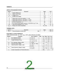
(refer to the test circuits, VS = 35V, Tamb = 25oC unless otherwise specified)
Symbol
Parameter
Pin 2 Quiescent Current
Test Conditions
I3 = 0, I5 = 0
Min. Typ. Max. Unit Fig.
I2
I6
I1
8
16
36
mA 1a
mA 1a
Pin 6 Quiescent Current
I3 = 0, I5 = 0
16
Amplifier Input Bias Current
V1 = 1 V, V7 = 2 V
V1 = 2 V, V7 = 1 V
I3 = 20 mA
– 0.1 – 1
– 0.1 – 1
µA
µA
V
1a
1a
1c
1d
1c
1c
1b
1b
V3L
V5
Pin 3 Saturation Voltage to GND
Quiescent Output Voltage
1
1.5
Vs = 35V, Ra = 39 kΩ
I5 = 1.2 A
18
V
V5L
Output Saturation Voltage to GND
1
1.4
1
V
I5 = 0.7 A
0.7
1.6
1.3
140
V
V5H
Tj
Output Saturation Voltage to Supply
– I5 = 1.2 A
2.2
1.8
V
– I5 = 0.7 A
V
Junction Temperature for Thermal Shut Down
°C
2/5

 STMICROELECTRONICS [ ST ]