Application hints
TDA7850
4
Application hints
Ref. to the circuit of Figure 2.
4.1
SVR
Besides its contribution to the ripple rejection, the SVR capacitor governs the turn ON/OFF
time sequence and, consequently, plays an essential role in the pop optimization during
ON/OFF transients. To conveniently serve both needs, Its minimum recommended value
is 10µF.
4.2
4.3
Input stage
The TDA7850's inputs are ground-compatible and can stand very high input signals (
8Vpk) without any performance degradation.
If the standard value for the input capacitors (0.1µF) is adopted, the low frequency cut-off
will amount to 16 Hz.
Stand-by and muting
STAND-BY and MUTING facilities are both CMOS compatible. In absence of true CMOS
ports or microprocessors, a direct connection to Vs of these two pins is admissible but a
470kΩ equivalent resistance should be present between the power supply and the muting
and stand-by pins.
R-C cells have always to be used in order to smooth down the transitions for preventing any
audible transient noises.
About the stand-by, the time constant to be assigned in order to obtain a virtually pop-free
transition has to be slower than 2.5V/ms.
4.4
4.5
DC offset detector
The TDA7850 integrates a DC offset detector to avoid an anomalous DC offset on the inputs
of the amplifier which may be multiplied by the gain, and result in a dangerous large offset
on the outputs, which may lead to speaker damage through overheating.
The feature is enabled by the MUTE pin and works with the amplifier unmuted and with no
signal on the inputs. The DC offset detection is signaled out on the HSD pin.
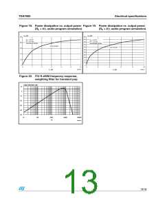
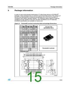
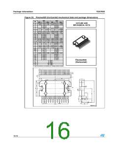
Heatsink definition
Under normal usage (4 Ohm speakers) the heatsink's thermal requirements have to be
deduced from Figure 18, which reports the simulated power dissipation when real
music/speech programmes are played out. Noise with gaussian-distributed amplitude was
employed for this simulation. Based on that, frequent clipping occurrence (worst-case) will
cause P
= 26W. Assuming T
= 70°C and T
= 150°C as boundary conditions, the
diss
amb
CHIP
heatsink's thermal resistance should be approximately 2°C/W. This would avoid any thermal
shutdown occurrence even after long-term and full-volume operation.
14/18

 STMICROELECTRONICS [ ST ]