TDA7454
can deliver. This holds true even at high volumes
and frequent clipping occurrence.
OPERATING PRINCIPLE.
Thanks to its unique operating principle, the
TDA7454 obtains a substantialreduction of power
dissipation from traditional class-AB amplifiers
without being affected by the massive radiation
effects and complex circuitry normally associated
with class-D solutions.
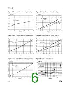
Applied to the TDA7454 (rated power= 25 W),
this will result into an average output level of 2.5
- 3 W in sine-wave operation, region where the
dissipated power is about 50 % less than that of a
traditional amplifier of equivalentpower class (see
TDA7454 vs. CLASS-AB characteristics, fig. 18).
Equally favourable is the case shown by fig. 19,
when gaussian-distributed signal amplitudes,
which best simulates the amplifier’s real working
conditions, are used.
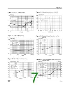
Its is composed of 8 amplifier blocks, making up
4 bridge-equivalent channels. Half of this struc-
ture is drafted in fig 15. These blocks continu-
ously change their connections during every sin-
gle signal event, according to the instantaneous
power demand. This means that at low volumes
(output power steadily lower than 2.5 W) the
TDA7454 acts as a Single Ended amplifier, condi-
tion where block “C” remains disabled and the
block “D” behaves like a buffer, which, by furnish-
ing the correct DC biasing (half-Vcc) to each pair
of speakers, eliminate the needs of otherwise re-
quired output-decoupling capacitors. At the same
time, SW1 keeps closed. thus ensuring a com-
mon biasing point for L-R front / L-R rear speak-
ers couples. As a result, the equivalent circuit be-
comes that of fig. 16.
The internal switches (SW1) are high-speed, dis-
sipation-free power MOS types, whose realization
has been made possible by the ST- exclusive By-
polar-CMOS-DMOS mixed technology process
(BCD). From fig. 16 it can be observed that “A”
and “B” amplifiers work in phase opposition. Sup-
posing their output have the same signal (equal
shape/amplitude), the current sourced by “B” will
be entirely sunk by “A”, while no current will flow
into “D”, causing no power dissipation in the lat-
ter.
“A” and “B” are practically configured as a bridge
whose load is constitutedby Ra + Rb (= 8 Ohm, if
4 Ohm speakers are used), with considerable ad-
vantages in terms of power dissipation. Designat-
ing “A” and “B” for the reproduction of either
FRONT or REAR sections of the same channel
(LEFT or RIGHT), keeping the fader in centre po-
sition (same amplitude for FRONT and REAR
sections) and using the same speakers, as it hap-
pens during most of the time, will transpose this
best-case dissipation condition into practical ap-
plications.
To fully take advantageof the TDA7454’s low-dis-
sipation feature, it is then especially important to
adopt some criteria in the channels assignment,
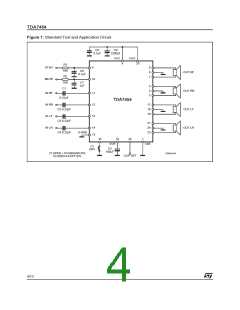
using the schematic of fig. 1 as a reference.
When the power demand increases to more than
2.5 W, all the blocks will operate as amplifiers,
SW1 is opened, leading to the seemingly conven-
tional bridge configuration of fig. 17.
APPLICATION HINTS (ref. to the circuit of fig. 1)
STAND-BY and MUTING (pins 4 & 22)
Both STAND-BY and MUTING pins are CMOS-
compatible. The current sunk by each of them is
about 1 µA. For pop prevention it is essential that
during TURN ON/OFF sequences the muting be
preventively inserted before making stand-by
transitions. But, if for any reason, either muting or
stand-by are not used, they have to be connected
to Vcc through a 100 Kohm (minimum) resis-
tance.
The R-C networks values in fig. 1 (R1-C6 and R2-
C7) are meant to be the minimum-necessary for
obtaining the lowest pop levels possible. Any re-
ductions (especially for R2-C7) will inevitably im-
pair this parameter.
SVR (pin 10)
The duty of the SVR capacitor (C5) is double: as-
suring adequate supply-ripple rejection and con-
trolling turn ON/OFF operations. Its indicated
value (100 uF) is the minimum-recommended to
correctly serve both the purposes.
INPUTS (pins 11-12-13-14)
The inputs are internally biased at half-Vcc level.
The typical input impedance is 15 KOhm, which
implies using Cin (C1-C2-C3-C4) = 220 nF for ob-
taining a theoretical minimum-reproducible fre-
quency of 48 Hz (-3 dB). In any case, Cin val-
ues can be enlarged if a lower frequency bound
is desired, but, at any Cin enlargement must cor-
respond a proportional increase of Csvr (C5), to
safeguard the on/off pop aspect.
The following table indicates the right values to be
used for Cin and Csvr, whose operating voltage
can be 10 V.
LOW FREQUENCY
ROLL-OFF (-3dB)
Cin (µF)
Csvr (µF)
48
22
16
11
0.22
0.47
0.68
1
100
220
330
470
The efficiency enhancement is based upon the
concept that the average output power during the
reproduction of normal music/speech programs
will stand anywhere between 10 % and 15 % of
the rated power (@ THD= 10 %) that the amplifier
8/13

 STMICROELECTRONICS [ ST ]