TDA7454
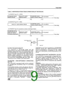
TAB (pin 1) is connected to the chip substrate
and has to be grounded to the best-filtered
ground spot (usually nearby the minus terminal of
the Vcc-filtering electrolytic capacitor). This same
point should be used as the centre of a multi-track
star-like configuration, or, alternatively, as the ori-
gin of only two separate tracks, one for P-GND,
one for S-GND, each of them routed to their spe-
cific ground pin(s).
This will provide the right degree of separation
between P-GND and S-GND yet assuring the
(necessary) electrical connection between them.
The correct ground assignment for the each ele-
ment of the circuit will then be:
This constitues a substantial difference from the
“clipping” situation, making the two information
unmistakable. Associated to a suitable external
circuitry, this “warning” signal could be used to
mute some portions of the I.C. (e.g. the rear
channels) or to attenuatethe volume.
Short Circuit
Some kinds of short circuit (OUT - GND, OUT-
Vcc), either present before the power-on or made
afterwards, will cause pin 25 to remain steadily
low as long as the faulty condition persists.
Short-circuits across the speakers will give inter-
mittent (pulsed) signalling, proportional to the
output voltage amplitude.
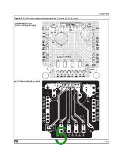
POWER GND:
Battery (-), Supply filters (C8, C9), TAB (pin 1).
External Layout Grounding
The 4 bridge stuctures have independent power
ground accesses (pins 2,8,18,24), while the sig-
nal ground is common to all of them(pin 13). The
SIGNAL GND:
Pre-amplifier (Audiprocessor) ground, SVR ca-
pacitor (C5), muting/st-bycapacitors (C6, C7).
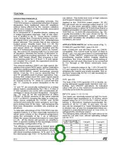
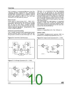
Figure 15: TDA7454’sHalf Structure
Figure 16: Single Ended Operation (Po < 2.5W)
+
-
A
B
+
-
RF
RR
INF
A
B
INR
RF
RR
INF
INR
SW1
Vf
Vr
C
D
-
+
Ron2
D
-
if
+
if-ir
F-channel
R-channel
D97AU793
CONTROL
LOGIC
D97AU792
Figure 17: He Bridge Operation(Po < 2.5W)
+
-
INF
A
C
B
D
INR
RF
RR
Vf
Vr
-
+
D97AU794
10/13

 STMICROELECTRONICS [ ST ]