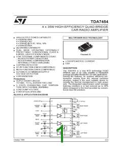
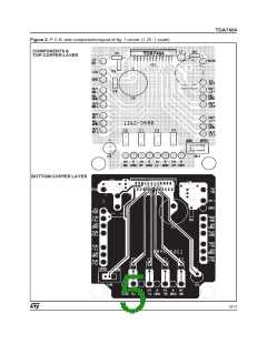
TDA7454
Ω
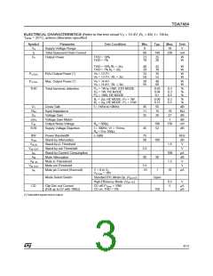
ELECTRICAL CHARACTERISTICS (Refer to the test circuit VS = 14.4V; RL = 4 ; f = 1KHz;
T
amb = 25°C, unless otherwise specified
Symbol
Parameter
Supply Voltage Range
Total Quiescent Drain Current
Output Power
Test Condition
Min.
8
Typ.
Max.
Unit
V
VS
Id
18
60
140
250
mA
Po
THD = 10%
THD = 1%
23
18
25
20
W
W
THD = 10% RL = 2Ω;
40
28
42
30
W
W
THD = 1% R = 2 ;
Ω
L
Po EIAJ
Po max.
THD
EIAJ Output Power (*)
Max. Output Power (*)
Total harmonic distortion
Vs = 13.7V
Vs = 13.7V, RL = 2Ω
32
50
35
52
W
W
Vs = 14.4V
Vs = 14.4V, RL = 2
38
55
40
60
W
W
Ω
P
P
P
O = 1W to 10W; STD MODE
O = 1W; HE MODE
O = 10W; HE MODE
0.03
0.04
0.1
0.3
0.3
0.5
%
%
%
RL = 2Ω; HE MODE; PO = 3W
0.06
0.15
0.3
0.5
%
%
R = 2 ; HE MODE; PO = 15W
Ω
L
CT
RIN
GV
Cross Talk
f = 1KHz to 10KHz
45
11
25
55
15
26
dB
KΩ
dB
dB
mV
dB
Input Impedance
Voltage Gain
19
27
1
G
Voltage Gain Match
Output Noise Voltage
Supply Voltage Rejection
∆
V
EIN
R = 600
100
52
150
Ω
g
SVR
f = 300Hz; Vr = 1Vrms;
45
Rg = 0 to 100Ω;
BW
ASB
Power Bandwidth
(–3dB)
75
90
KHz
dB
V
Stand-by Attenuation
Stand-by in Threshold
Stand-by out Threshold
Stand-by Current Consumption
Mute Attenuation
100
90
Vsb IN
Vsb OUT
Isb
1.5
100
1.5
10
3.5
80
V
µA
dB
V
AM
VM
Mute in Thereshold
IN
VM OUT
IM
Mute out Threshold
3.5
-10
V
Mute pin Current (Sourced)
V = 0 to VS
1
µA
VS max = 18V
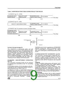
Mode Select Switch
Standard BTL Mode Op. (Vpin16
)
Open
High Efficiency Mode (Vpin 16
)
0.5
5
V
CD
Clip Det. out Current
CD off: POmin = 10W
CD on: THD = 5%
A
µ
µA
(Pull up to 5V with 10KΩ)
150
(*) Saturated square wave output.
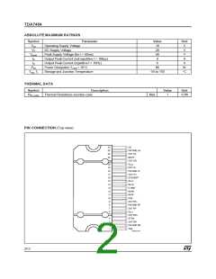
3/13

 STMICROELECTRONICS [ ST ]