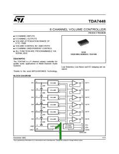
TDA7448
2
I C BUS INTERFACE
2
Data transmission from microprocessor to the TDA7448 and vice versa takes place through the 2 wires I C BUS in-
terface, consisting of the two lines SDA and SCL (pull-up resistors to positive supply voltage must be connected).
Data Validity
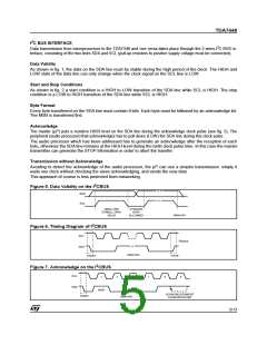
As shown in fig. 1, the data on the SDA line must be stable during the high period of the clock. The HIGH and
LOW state of the data line can only change when the clock signal on the SCL line is LOW.
Start and Stop Conditions
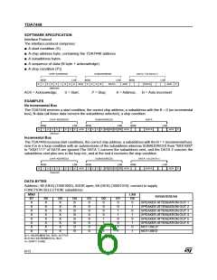
As shown in fig. 2 a start condition is a HIGH to LOW transition of the SDA line while SCL is HIGH. The stop
condition is a LOW to HIGH transition of the SDA line while SCL is HIGH.
Byte Format
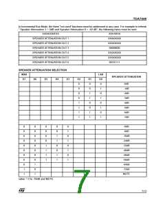
Every byte transferred on the SDA line must contain 8 bits. Each byte must be followed by an acknowledge bit.
The MSB is transferred first.
Acknowledge
The master (µP) puts a resistive HIGH level on the SDA line during the acknowledge clock pulse (see fig. 5). The
peripheral (audio processor) that acknowledges has to pull-down (LOW) the SDA line during this clock pulse.
The audio processor which has been addressed has to generate an acknowledge after the reception of each
byte, otherwise the SDA line remains at the HIGH level during the ninth clock pulse time. In this case the master
transmitter can generate the STOP information in order to abort the transfer.
Transmission without Acknowledge
Avoiding to detect the acknowledge of the audio processor, the µP can use a simpler transmission: simply it
waits one clock without checking the slave acknowledging, and sends the new data.
This approach of course is less protected from misworking.
2
Figure 5. Data Validity on the I CBUS
SDA
SCL
DATA LINE
STABLE, DATA
VALID
CHANGE
DATA
ALLOWED
D99AU1031
2
Figure 6. Timing Diagram of I CBUS
SCL
2
I CBUS
SDA
D99AU1032
START
STOP
2
Figure 7. Acknowledge on the I CBUS
SCL
1
2
3
7
8
9
SDA
MSB
ACKNOWLEDGMENT
FROM RECEIVER
START
D99AU1033
5/13

 STMICROELECTRONICS [ ST ]