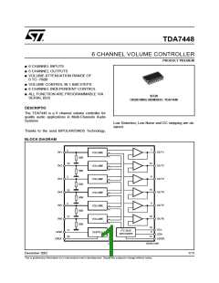
TDA7448
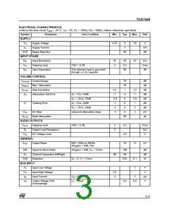
ELECTRICAL CHARACTERISTCS
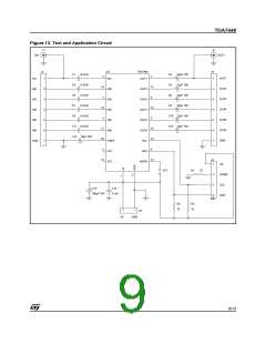
(refer to the test circuit T = 25°C, V = 9V, R = 10K
Ω
, R = 600Ω, unless otherwise specified)
G
amb
Parameter
S
L
Symbol
Test Condition
Min.
Typ.
Max.
Unit
SUPPLY
V
Supply Voltage
4.75
9
7
10
65
V
S
I
Supply Current
Ripple Rejection
mA
dB
S
SVR
80
INPUT STAGE
R
Input Resistance
Clipping Level
35
2
50
2.5
90
KΩ
Vrms
dB
IN
V
CL
THD = 0.3%
S
IN
Input Separation
The selected input is grounded
through a 2.2µ capacitor
VOLUME CONTROL
C
Control Range
79
79
1
dB
dB
dB
dB
dB
dB
dB
mV
db
RANGE
A
Max. Attenuation
Step Resolution
Attenuation Set Error
VMAX
A
0.5
-1
1.5
1
STEP
E
A = 0 to -24dB
0
A
T
V
A = -24 to -79dB
V
-2.0
-1
0
2.0
1
E
Tracking Error
A = 0 to -24dB
V
0
A = -24 to -79dB
V
-2
0
2
V
DC Step
adyacent attenuation steps
THD = 0.3%
-3
0
3
DC
A
Mute Attenuation
90
mute
AUDIO OUTPUTS
V
Clipping Level
2
2
2.5
4.5
10
Vrms
KΩ
V
CLIP
R
Output Load Resistance
DC Voltage Level
L
V
DC
GENERAL
E
Output Noise
BW = 20Hz to 20KHz
All gains = 0dB, Flat
15
µV
NO
S/N
Signal to Noise Ratio
Channel Separation left/Right
Distortion
All gains = 0dB; V = 1Vrms
100
90
dB
dB
%
O
S
C
80
THD
BUS INPUT
A = 0; V = 1Vrms
0.01
0.1
1
V
I
V
Il
Input Low Voltage
Input High Voltage
Input Current
V
V
V
IH
2.5
-5
I
IN
V
= 0.4V
5
µA
V
IN
V
O
Output Voltage SDA
Achnowledge
I
= 1.6mA
O
0.4
0.8
3/13

 STMICROELECTRONICS [ ST ]