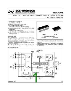
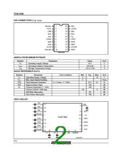
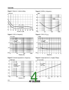
TDA7309
THERMAL DATA
Symbol
Parameter
Thermal resistance Junction to Pins
SO20
DIP20
Unit
Rth j-pins
150
100
C/W
°
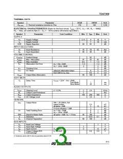
ELECTRICAL CHARACTERISTICS (Refer to the test circuit, Tamb = 25°C, VS = 9V, RL = 10KΩ,
RG = 50Ω, all controls flat (G = 0), f = 1KHzunless otherwise specified.)
Symbol
Parameter
Test Condition
Min.
Typ.
Max.
Unit
SUPPLY
VS
IS
SVR
Supply Voltage
5 (*)
60
9
7
85
10
10
V
Supply Current
Ripple Rejection
mA
dB
INPUT SELECTORS
RI
Sin
Input Resistance
Input Separation
35
80
50
90
65
KΩ
dB
VOLUME CONTROL
CRANGE
AVMAX
ASTEP
EA
Control Range
Max. Attenuation
Step resolution
92
92
1
dB
dB
dB
dB
dB
dB
mV
mV
dB
87
0.5
-1.2
-3
95
1.5
1.2
2
Attenuation Set Error
AV = 0 to -24dB
AV = -24 to -56dB
ET
Tracking Error
DC Steps
2
VDC
adjacent attenuation steps
from 0dB to AV max.
0
0.5
100
3
5
Amute
SOFT MUTE
Td
Output Mute Attenuation
Delay Time
80
Csmute = 22nF 0 to –20dB
Fast Mode
Slow Mode
1
20
ms
ms
AUDIO OUTPUTS
VCLIP
RL
Rout
VDC
Clipping Level
d = 0.3%
2
2
100
2.6
Vrms
KΩ
Ω
Output Load Resistance
Output Impedance
DC Voltage Level
200
3.8
300
15
V
GENERAL
eNO
Output Noise
BW = 20-20KHz, flat
output muted
all gains = 0dB
2.5
5
µV
V
µ
A curve all gains = 0dB
3
µV
Et
Total Tracking Error
AV = 0 to –24dB
AV = -24 to –56dB
0
0
1
2
dB
dB
S/N
d
SC
Signal to Noise Ratio
Distortion
Channel Separation
all gains = 0dB; VO = 1Vrms
95
80
106
0.01
100
dB
%
dB
0.1
BUS INPUTS
VIL
VIH
IIN
Input Low Voltage
Input High Voltage
Input Current
1
V
V
A
µ
3
-5
Vin = 0.4V
IO = 1.6mA
+5
VO
Output Voltage SDA
Acknowledge
0.4
0.8
V
(*) Hedevice work until 5V but no guarantee about SVR
3/12

 STMICROELECTRONICS [ ST ]