TDA7294
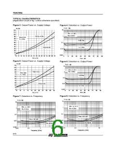
Figure 16: Turn ON/OFF Suggested Sequence
+Vs
(V)
+35
-35
-Vs
V
(mV)
IN
V
ST-BY
5V
5V
PIN #9
(V)
V
MUTE
PIN #10
(V)
I
P
(mA)
V
OUT
(V)
OFF
ST-BY
PLAY
ST-BY
OFF
MUTE
MUTE
D93AU013
Tj = 150 oC).
Full protection against electrostatic discharges on
every pin is included.
In addition to the overload protection described
above, the device features a thermal shutdown
circuit which initially puts the device into a muting
state (@ Tj = 145 oC) and then into stand-by (@
3) Other Features
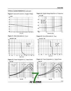
Figure 17: Single Signal ST-BY/MUTE Control
Circuit
The device is provided with both stand-by and
mute functions, independently driven by two
CMOS logic compatibleinput pins.
The circuits dedicated to the switching on and off
of the amplifier have been carefully optimized to
avoid any kind of uncontrolled audible transient at
the output.
The sequence that we recommend during the
ON/OFF transients is shown by Figure 16.
MUTE
STBY
20K
30K
MUTE/
ST-BY
10K
The application of figure 17 shows the possibility
of using only one command for both st-by and
mute functions. On both the pins, the maximum
applicable range corresponds to the operating
supply voltage.
10µF
10µF
1N4148
D93AU014
9/16

 STMICROELECTRONICS [ ST ]