TDA7294
APPLICATION INFORMATION
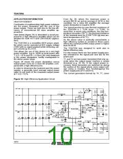
HIGH-EFFICIENCY
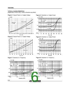
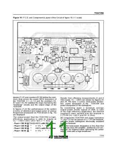
From fig. 20, where the maximum power is
around 200 W, we get an average of 20 W, in this
condition, for a class AB amplifier the average
power dissipation is equal to 65 W.
Constraints of implementing high power solutions
are the power dissipation and the size of the
power supply. These are both due to the low effi-
ciency of conventional AB class amplifier ap-
proaches.
The typical junction-to-case thermal resistance of
o
o
the TDA7294 is 1 C/W (max= 1.5 C/W). To
avoid that, in worst case conditions, the chip tem-
perature exceedes 150 oC, the thermal resistance
of the heatsink must be 0.038 oC/W (@ max am-
bient temperature of 50 oC).
Here below (figure 18) is described a circuit pro-
posal for a high efficiency amplifier which can be
adopted for both HI-FI and CAR-RADIO applica-
tions.
The TDA7294 is a monolithic MOS power ampli-
fier which can be operated at 80V supply voltage
(100V with no signal applied) while delivering out-
put currents up to ±10 A.
As the above value is pratically unreachable; a
high efficiency system is needed in those cases
where the continuousRMS output power is higher
than 50-60 W.
The TDA7294 was designed to work also in
higher efficiency way.
This allows the use of this device as a very high
power amplifier (up to 180W as peak power with
T.H.D.=10 % and Rl = 4 Ohm); the only drawback
is the power dissipation, hardly manageable in
the above power range.
Figure 20 shows the power dissipation versus
output power curve for a class AB amplifier, com-
pared with a high efficiency one.
In order to dimension the heatsink (and the power
supply), a generally used average output power
value is one tenth of the maximum output power
at T.H.D.=10 %.
For this reason there are four power supply pins:
two intended for the signal part and two for the
power part.
T1 and T2 are two power transistors that only op-
erate when the output power reaches a certain
threshold (e.g. 20 W). If the output power in-
creases, these transistors are switched on during
the portion of the signal where more output volt-
age swing is needed, thus ”bootstrapping” the
power supply pins (#13 and #15).
The current generators formed by T4, T7, zener
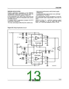
Figure 18: High Efficiency Application Circuit
+40V
T3
BC394
R4
270
R5
270
T1
BDX53A
D1 BYW98100
T4
BC393
T5
BC393
+20V
270
L1 1µH
D3 1N4148
R6
20K
C11 330nF
Z1 3.9V
C11 22µF
7
13
C1
1000µF
C3
100nF
C5
1000µF
C7
100nF
C9
330nF
IN
3
R3 680
R16
13K
2
R7
C16
3.3K
1.8nF
R1
2
R16
L3 5µH
4
9
13K
TDA7294
PLAY
14
OUT
C13 10µF
GND
270
C15
22µF
R13 20K
R14 30K
R15 10K
ST-BY
6
1
R8
3.3K
C17
1.8nF
R2
2
D5
1N4148
8
15
C2
C4
C6
C8
C10
330nF
10
Z2 3.9V
1000µF
100nF
1000µF
100nF
C14
10µF
L2 1µH
D4 1N4148
T7
T8
BC394
BC394
D2 BYW98100
270
-20V
T2
BDX54A
R9
270
R10
270
R11
29K
T6
BC393
-40V
D93AU016
10/16

 STMICROELECTRONICS [ ST ]