TDA7294
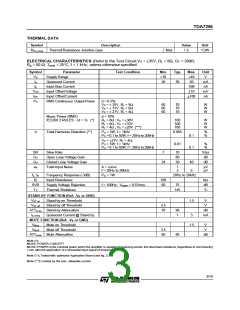
THERMAL DATA
Symbol
Description
Thermal Resistance Junction-case
Value
Unit
Rth j-case
Max
1.5
°C/W
ELECTRICAL CHARACTERISTICS (Refer to the Test Circuit VS = ±35V, RL = 8Ω, GV = 30dB;
Rg = 50 Ω; Tamb = 25°C, f = 1 kHz; unless otherwise specified.
Symbol
VS
Parameter
Supply Range
Test Condition
Min.
±10
20
Typ.
Max.
±40
60
Unit
V
Iq
Quiescent Current
30
mA
nA
Ib
Input Bias Current
500
+10
+100
VOS
IOS
Input Offset Voltage
Input Offset Current
RMS Continuous Output Power
mV
nA
PO
d = 0.5%:
VS = ± 35V, RL = 8Ω
VS = ± 31V, RL = 6Ω
VS = ± 27V, RL = 4Ω
60
60
60
70
70
70
W
W
W
Music Power (RMS)
d = 10%
IEC268.3 RULES - ∆t = 1s (*)
RL = 8
RL = 6
RL = 4
Ω
Ω
Ω
; VS = ±38V
; VS = ±33V
; VS = ±29V (***)
100
100
100
W
W
W
d
Total Harmonic Distortion (**)
P
O = 5W; f = 1kHz
0.005
%
%
PO = 0.1 to 50W; f = 20Hz to 20kHz
0.1
0.1
VS = ±27V, RL = 4Ω:
O = 5W; f = 1kHz
O = 0.1 to 50W; f = 20Hz to 20kHz
P
P
0.01
%
%
SR
GV
GV
eN
Slew Rate
7
10
80
30
V/µs
dB
Open Loop Voltage Gain
Closed Loop Voltage Gain
Total Input Noise
24
40
5
dB
A = curve
f = 20Hz to 20kHz
1
2
µV
µV
fL, fH
Ri
Frequency Response (-3dB)
Input Resistance
PO = 1W
20Hz to 20kHz
100
60
kΩ
dB
°C
SVR
TS
Supply Voltage Rejection
Thermal Shutdown
f = 100Hz; Vripple = 0.5Vrms
75
145
STAND-BY FUNCTION (Ref: -VS or GND)
VST on
VST off
Stand-by on Threshold
Stand-by off Threshold
1.5
V
V
3.5
70
ATTst-by Stand-by Attenuation
90
dB
mA
Iq st-by
Quiescent Current @ Stand-by
1
3
MUTE FUNCTION (Ref: -VS or GND)
VMon
VMoff
Mute on Threshold
Mute off Threshold
1.5
V
V
3.5
60
ATTmute Mute AttenuatIon
80
dB
Note (*):
MUSIC POWER CONCEPT
MUSIC POWER is the maximal power which the amplifier is capable of producing across the rated load resistance (regardless of non linearity)
1 sec after the application of a sinusoidal input signal of frequency 1KHz.
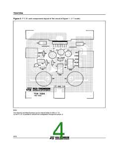
Note (**): Tested with optimized Application Board (see fig. 2)
Note (***): Limited by the max. allowable current.
3/16

 STMICROELECTRONICS [ ST ]