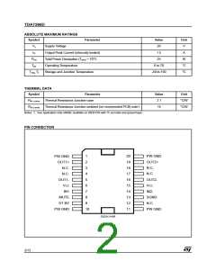
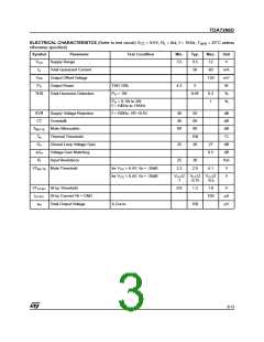
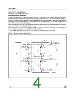
TDA7266D
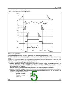
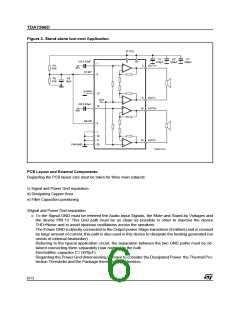
Figure 3. Stand-alone low-cost Application
V
CC
C1
470µF
C2
100nF
C7
100nF
C3 0.22µF
6
15
7
R1
47K
+
-
2
OUT1+
IN1
ST-BY
9
R2
C4
47K
10µF
S-GND
13
Vref
-
5
OUT1-
OUT2+
+
C5 0.22µF
14
+
-
19
IN2
MUTE
8
1
10
11
20
-
16
OUT2-
PW-GND
+
D02AU1410
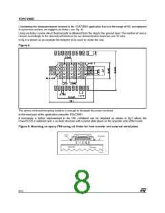
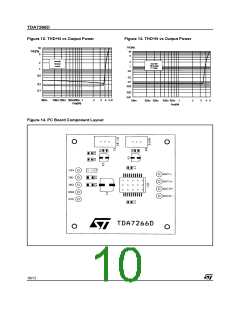
PCB Layout and External Components:
Regarding the PCB layout care must be taken for three main subjects:
c) Signal and Power Gnd separation
d) Dissipating Copper Area
e) Filter Capacitors positioning
)Signal and Power Gnd separation:
c To the Signal GND must be referred the Audio Input Signals, the Mute and Stand-by Voltages and
the device PIN.13. This Gnd path must be as clean as possible in order to improve the device
THD+Noise and to avoid spurious oscillations across the speakers.
The Power GND is directly connected to the Output power Stage transistors (Emitters) and is crossed
by large amount of current, this path is also used in this device to dissipate the heating generated (no
needs of external heatsinker).
Referring to the typical application circuit, the separation between the two GND paths must be ob-
tained connecting them separately (star routing) to the bulk
Electrolithic capacitor C1 (470µF).
Regarding the Power Gnd dimensioning we have to consider the Dissipated Power the Thermal Pro-
tection Threshold and the Package thermal Characteristics.
6/13

 STMICROELECTRONICS [ ST ]