TDA2030A
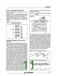
APPLICATION SUGGESTION
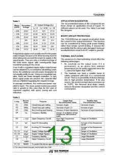
Table 1
The recommended values of the components are
those shown on application circuit of Figure 14.
Different values can be used. The Table2 can help
the designer.
DC Output Voltage (Vo)
Io = 0 Io = 0.1A Io = 1A
Mains Secondary
(220V)
Voltage
+ 20%
+ 15%
+ 10%
–
28.8V
27.6V
26.4V
24V
43.2V
41.4V
39.6V
36.2V
32.4V
30.6V
28.8V
42V
40.3V
38.5V
35V
37.5V
35.8V
34.2V
31V
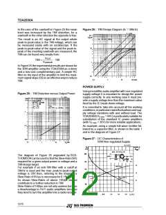
SHORT CIRCUIT PROTECTION
The TDA2030Ahas an original circuit which limits
the current of the output transistors. This function
can be considered as being peak power limiting
rather than simple current limiting. It reduces the
possibility that the device gets damaged during an
accidental short circuit from AC output to ground.
– 10%
– 15%
– 20%
21.6V
20.4V
19.2V
31.5V
29.8V
28V
27.8V
26V
24.3V
Aregulatedsupplyis not usuallyused for thepower
output stagesbecause of its dimensioning must be
done taking into account the power to supply in the
signal peaks. They are only a small percentage of
the total music signal, with consequently large
overdimensioningof the circuit.
Even if with a regulatedsupply higheroutput power
can be obtained (VS is constant in all working condi-
tions), the additional cost and power dissipation do
not usually justify its use. Using non-regulated sup-
plies, there are fewer designe restriction. In fact,
when signal peaks are present, the capacitor filter
acts as a flywheel supplying the required energy.
THERMAL SHUT-DOWN
The presenceof a thermal limiting circuit offers the
following advantages:
1. An overload on the output (even if it is
permanent), or an above limit ambient
temperaturecan be easily supported since the
Tj cannot be higher than 150oC.
2. The heatsink can have a smaller factor of
safety compared with that of a conventional
circuit. There is nopossibility of devicedamage
due to high junction temperature. If for any
reason, the junction temperatureincreases up
to 150oC, the thermal shut-down simply
reduces the power dissipation and the current
consumption.
In average conditions, the continuous power sup-
plied is lower. The music power/continuouspower
ratio is greater in this case than for the case of
regulated supplied, with space saving and cost
reduction.
Table 2
Recom.
Larger than
Smaller than
Comp.
Purpose
Value
22kΩ
680Ω
22kΩ
1Ω
Recommended Value
Recommended Value
R1
R2
R3
R4
Closed loop gain setting
Closed loop gain setting
Non inverting input biasing
Frequency Stability
Increase of gain
Decrease of gain
Decrease of gain (*)
Increase of input impedance
Increase of gain
Decrease of input impedance
Danger of oscillation at high
frequencies with inductive
loads
R5
C1
C2
Upper Frequency Cut-off
Input DC Decoupling
Poor High Frequencies
Attenuation
Danger of Oscillation
3 R2
1µF
Increase of low frequencies
cut-off
Inverting DC Decoupling
Increase of low frequencies
cut-off
22µF
C3, C4
C5, C6
C7
Supply Voltage Bypass
Supply Voltage Bypass
Frequency Stability
Danger of Oscillation
Danger of Oscillation
Larger Bandwidth
Larger Bandwidth
0.1µF
100µF
0.22µF
1
C8
Upper Frequency Cut-off
Smaller Bandwidth
≈
2πBR1
D1, D2
1N4001
To protect the device against output voltage spikes
(*) The value of closed loop gain must be higher than 24dB.
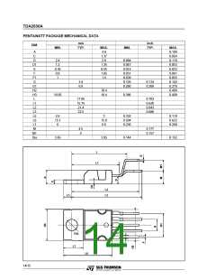
13/15

 STMICROELECTRONICS [ ST ]