TDA2006
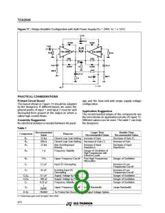
SHORT CIRCUIT PROTECTION
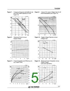
Figure 19 : Safe Operating Area and Collector
Characteristics of the Protected
Power Transistor
The TDA2006 has an original circuit which limits
the current of the output transistors. Figure 18
shows that the maximum output current is a func-
tion of the collector emitter voltage ; hence the
output transistors work within their safe operating
area (Figure 19).
This functioncan thereforebe considered as being
peak power limiting rather than simple current lim-
iting.
It reduces the possibility that the device gets dam-
aged during an accidental short circuit from AC
output to ground.
THERMAL SHUT DOWN
The presence of a thermal limiting circuit offers the
following advantages :
1) an overload on the output (even if it is
permanent), or an above limit ambient
temperature can be easily supported since the
Tj cannot be higher than 150°C.
Figure 20 : Output Power and Drain Current ver-
sus Case Temlperature (RL = 4Ω)
2) the heatsink can have a smaller factor of safety
compared with that of a conventional circuit.
There is no possibility of device damage due to
high junction temperature.
If for any reason, the junction temperature in-
creases up to 150 °C, the thermalshutdown simply
reduces the power dissipation andthe current con-
sumption.
The maximum allowable power dissipation de-
pends upon the size of the external heatsink (i.e.
its thermal resistance) ; Figure 22 shows the dissi-
pable power as a function of ambient temperature
for different thermal resistances.
Figure 18 : Maximum Output Current versus
Voltage VCE (sat) accross each Out-
put Transistor
Figure 21 : Output Power and Drain Current ver-
sus Case Temlperature (RL = 8Ω)
9/12

 STMICROELECTRONICS [ ST ]