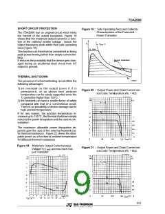
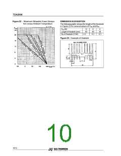
TDA2006
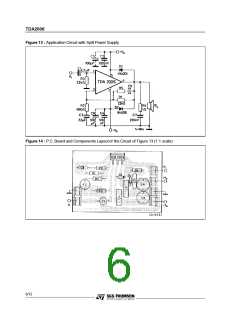
Figure 17 : Bridge Amplifier Configuration with Split Power Supply (PO = 24W, VS = ± 12V)
PRACTICAL CONSIDERATIONS
Printed Circuit Board
age and the heat-sink with single supply voltage
The layout shown in Figure 14 should be adopted
by the designers. If different layout are used, the
ground points of input 1 and input 2 must be well
decoupled from ground of the output on which a
rather high current flows.
configuration.
Application Suggestion
The recommended values of the components are
the ones shown on applicationcircuits of Figure13.
Different values can be used. The table 1 can help
the designers.
Assembly Suggestion
No electrical isolation is needed between the pack-
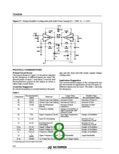
Table 1
Recommanded
Larger Than
Smaller Than
Component
Purpose
Value
22 kΩ
680 Ω
22 kΩ
Recommanded Value
Recommanded Value
R1
R2
R3
Closed Loop Gain Setting Increase of Gain
Closed Loop Gain Setting Decrease of Gain (*)
Decrease of Gain (*)
Increase of Gain
Non Inverting Input
Biasing
Increase of Input
Impedance
Decrease of Input
Impedance
R4
1 Ω
Frequency Stability
Danger of Oscillation at
High Frequencies with
Inductive Loads
R5
C1
C2
3 R2
2.2 µF
22 µF
Upper Frequency Cut-off
Input DC Decoupling
Poor High Frequencies
Attenuation
Danger of Oscillation
Increase of Low
Frequencies Cut-off
Inverting Input DC
Decoupling
Increase of Low
Frequencies Cut-off
C3C4
C5C6
C7
0.1 µF
100 µF
0.22 µF
Supply Voltage by Pass
Supply Voltage by Pass
Frequency Stability
Danger of Oscillation
Danger of Oscillation
Danger of Oscillation
1
C8
Upper Frequency Cut-off
Lower Bandwidth
Larger Bandwidth
2πBR1
D1D2
1N4001
To Protect the Device Against Output Voltage Spikes.
(*) Closed loop gain must be higher than 24dB.
8/12

 STMICROELECTRONICS [ ST ]