TDA1170S
ABSOLUTE MAXIMUM RATINGS
Symbol
Parameter
Value
35
Unit
V
VS
V4, V5
V10
Supply Voltage at Pin 2
Flyback Peak Voltage
60
V
Power Amplifier Input Voltage
+ 10
– 0.5
V
V
Io
Io
Output Peak Current (non repetitive) at t = 2msec
Output Peak Current at f = 50Hz t ≤ 10µsec
Output Peak Current at f = 50Hz t > 10µsec
Pin 3 DC Current at V4 2
2
A
A
2.5
1.5
100
1.8
± 20
Io
A
I3
mA
A
I3
Pin 3 Peak to Peak Flyback Current for f = 50Hz, tfly ≤ 1.5msec
Pin 8 Current
I8
mA
Ptot
Power Dissipation : at Ttab = 90 °C
at Tamb = 80 ° C
5
1
W
W
T
stg, Tj
Storage and Junction Temperature
– 40, + 150
°C
THERMAL DATA
Symbol
Parameter
Value
12
Unit
°C/W
°C/W
Rth j–tab
Thermal Resistance Junction–tab
Max
Max
Rth j–amb
Thermal Resistance Junction-ambient
70
(°) Obtained with tabs soldered to printed circuit with minimized copper area.
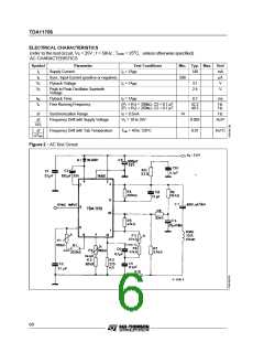
ELECTRICAL CHARACTERISTICS
(refer to the test circuits, VS = 35V, Tamb = 25°C, unless otherwise specified)
DC CHARACTERISTICS
Symbol
I2
Parameter
Pin 2 Quiescent Current
Pin 5 Quiescent Current
Oscillator Bias Current
Test Conditions
I3 = 0
Min. Typ. Max. Unit Fig.
7
8
14
15
1
mA
mA
µA
µA
µA
µA
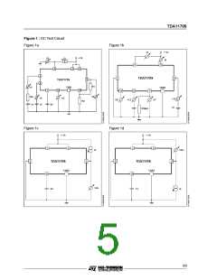
1b
1b
1a
1b
1a
1b
I5
I4 = 0
– I9
V9 = 1V
0.1
0.1
0.02
20
– I10
– I12
– I12
∆I12
I12
Amplifier Input Bias Current
Ramp Generator Bias Current
Ramp Generator Current
V10 = 1V
V12 = 0
1
0.3
24
I7 = 20 µA, V12 = 0
19
10
∆V12 = 0 to 12V, I7 =
20µA
Ramp Generator Non-linearity
0.2
1
%
1b
Vs
V1
V3
V4
Supply Voltage Range
35
1.4
V
V
V
V
–
–
Pin 1 Saturation Voltage to Ground
Pin 3 Saturation Voltage to Ground
Quiescent Output Voltage
I1 = 1 mA
1
I3 = 10 mA
1.7
4.4
2.6
1a
1a
VS = 10V
R1 = 10kΩ , R2 = 10kΩ
4.1
8.3
4.75
VS = 35V
R1 = 30kΩ, R2 = 10kΩ
8.8
9.45
V
1a
V4L
V4H
Output Saturation Voltage to Ground
Output Saturation Voltage to Supply
– I4 = 0.1A
– I4 = 0.8A
0.9
1.9
1.2
2.3
V
V
1c
1c
I4 = 0.1A
I4 = 0.8A
1.4
2.8
2.1
3.2
V
V
1d
1d
V6
V7
Regulated Voltage at Pin 6
Regulated Voltage at Pin 7
6.1
6.2
6.5
6.6
6.9
7
V
V
1b
1b
I7 = 20µA
∆V6 ∆V7
,
Regulated Voltage Drift with Supply
Voltage
∆VS = 10 to 35V
1
mV/V
1b
∆VS ∆VS
V10
R8
Amplifier Input Reference Voltage
Pin 8 Input Resistance
2.07
1
2.2
2.3
V
–
V8 ≤ 0.4V
MΩ
1a
4/9

 STMICROELECTRONICS [ ST ]