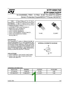
STP10NK70Z/STP10NK70ZFP
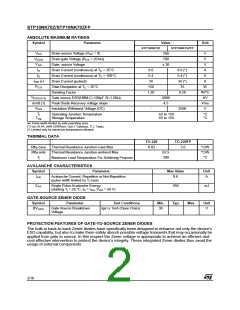
ELECTRICAL CHARACTERISTICS (TCASE =25°C UNLESS OTHERWISE SPECIFIED)
ON/OFF
Symbol
Parameter
Drain-source
Test Conditions
Min.
Typ.
Max.
Unit
V
I
= 1 mA, V = 0
700
V
(BR)DSS
D
GS
Breakdown Voltage
I
Zero Gate Voltage
V
V
= Max Rating
= Max Rating, T = 125 °C
1
50
µA
µA
DSS
DS
DS
Drain Current (V = 0)
GS
C
I
Gate-body Leakage
V
= ± 20V
±10
µA
GSS
GS
Current (V = 0)
DS
V
V
V
= V , I = 100µA
Gate Threshold Voltage
3
3.75
0.75
4.5
V
GS(th)
DS
GS
GS
D
R
Static Drain-source On
Resistance
= 10V, I = 4.5 A
0.85
Ω
DS(on)
D
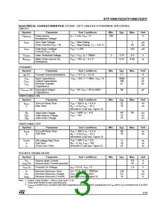
DYNAMIC
Symbol
Parameter
Test Conditions
Min.
Typ.
Max.
Unit
g
(1)
Forward Transconductance
V
V
= 15 V I = 4.5 A
7.7
S
fs
DS
, D
C
C
C
Input Capacitance
Output Capacitance
Reverse Transfer
Capacitance
V
= 25V, f = 1 MHz, V = 0
2000
190
41
pF
pF
pF
iss
DS
GS
oss
rss
C
(3) Equivalent Output
Capacitance
= 0V, V = 0V to 560V
98
pF
oss eq.
GS
DS
SWITCHING ON
Symbol
Parameter
Test Conditions
Min.
Typ.
Max.
Unit
t
Turn-on Delay Time
Rise Time
V
R
= 350 V, I = 4.5 A
= 4.7Ω V = 10 V
GS
22
19
ns
ns
d(on)
DD
D
t
r
G
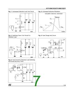
(Resistive Load see, Figure 3)
Q
Q
Q
V
V
= 560V, I = 9 A,
= 10V
64
12
33
90
Total Gate Charge
Gate-Source Charge
Gate-Drain Charge
nC
nC
nC
g
DD
GS
D
gs
gd
SWITCHING OFF
Symbol
Parameter
Test Conditions
Min.
Typ.
Max.
Unit
t
Turn-off Delay Time
Fall Time
V
= 350 V, I = 4.5 A
46
19
ns
ns
d(off)
DD
D
t
f
R = 4.7Ω V = 10 V
G GS
(Resistive Load see, Figure 3)
t
V
R
= 560 V, I = 9 A,
Off-voltage Rise Time
Fall Time
Cross-over Time
11
10
22
ns
ns
ns
r(Voff)
DD
D
t
f
= 4.7Ω, V = 10V
G
GS
t
c
(Inductive Load see, Figure 5)
SOURCE DRAIN DIODE
Symbol
Parameter
Test Conditions
Min.
Typ.
Max.
Unit
I
8.6
34
A
A
Source-drain Current
Source-drain Current (pulsed)
SD
(2)
I
SDM
V
(1)
I
I
= 8.6 A, V = 0
Forward On Voltage
1.6
V
SD
SD
SD
GS
t
= 9 A, di/dt = 100A/µs
= 35V, T = 150°C
Reverse Recovery Time
Reverse Recovery Charge
Reverse Recovery Current
720
5.4
15
ns
µC
A
rr
Q
V
DD
rr
RRM
j
I
(see test circuit, Figure 5)
Note: 1. Pulsed: Pulse duration = 300 µs, duty cycle 1.5 %.
2. Pulse width limited by safe operating area.
3. C
V
is defined as a constant equivalent capacitance giving the same charging time as C
when V increases from 0 to 80%
oss DS
oss eq.
.
DSS
3/10

 STMICROELECTRONICS [ ST ]