Electrical characteristics
STM32F105xx, STM32F107xx
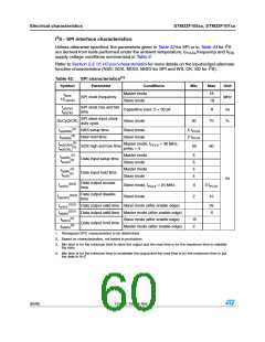
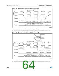
I2S - SPI interface characteristics
2
Unless otherwise specified, the parameters given in Table 42 for SPI or in Table 43 for I S
frequency and V
DD
are derived from tests performed under the ambient temperature, f
supply voltage conditions summarized in Table 9.
PCLKx
Refer to Section 5.3.12: I/O port characteristics for more details on the input/output alternate
2
function characteristics (NSS, SCK, MOSI, MISO for SPI and WS, CK, SD for I S).
(1)
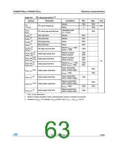
Table 42. SPI characteristics
Symbol
Parameter
Conditions
Master mode
Min
Max
Unit
18
18
fSCK
1/tc(SCK)
SPI clock frequency
MHz
Slave mode
tr(SCK)
tf(SCK)
SPI clock rise and fall
time
Capacitive load: C = 30 pF
8
ns
%
SPI slave input clock
duty cycle
DuCy(SCK)
Slave mode
30
70
(2)
tsu(NSS)
NSS setup time
NSS hold time
Slave mode
Slave mode
4 tPCLK
2 tPCLK
(2)
th(NSS)
(2)
tw(SCKH)
tw(SCKL)
Master mode, fPCLK = 36 MHz,
presc = 4
SCK high and low time
Data input setup time
50
60
(2)
(2)
Master mode
Slave mode
Master mode
Slave mode
5
5
5
4
tsu(MI)
tsu(SI)
(2)
(2)
th(MI)
th(SI)
Data input hold time
(2)
ns
Data output access
time
(2)(3)
ta(SO)
Slave mode, fPCLK = 20 MHz
Slave mode
0
2
3 tPCLK
Data output disable
time
(2)(4)
tdis(SO)
10
(2)(1)
tv(SO)
Data output valid time Slave mode (after enable edge)
Data output valid time Master mode (after enable edge)
25
5
(2)(1)
tv(MO)
(2)
th(SO)
Slave mode (after enable edge)
Data output hold time
Master mode (after enable edge)
15
2
(2)
th(MO)
1. Remapped SPI1 characteristics to be determined.
2. Based on characterization, not tested in production.
3. Min time is for the minimum time to drive the output and the max time is for the maximum time to validate
the data.
4. Min time is for the minimum time to invalidate the output and the max time is for the maximum time to put
the data in Hi-Z
60/95
Doc ID 15274 Rev 4

 STMICROELECTRONICS [ ST ]