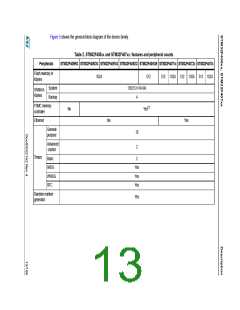
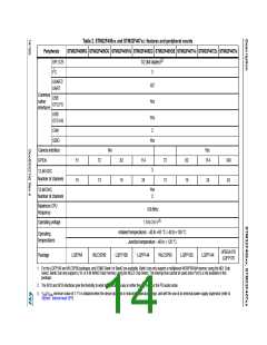
Table 2. STM32F405xx and STM32F407xx: features and peripheral counts
Peripherals
SPI / I2S
STM32F405RG STM32F405OG STM32F405VG STM32F405ZG STM32F405OE STM32F407Vx STM32F407Zx STM32F407Ix
3/2 (full duplex)(2)
3
I2C
USART/
UART
4/2
Yes
Yes
Communi
cation
interfaces
USB
OTG FS
USB
OTG HS
CAN
2
SDIO
Yes
Camera interface
GPIOs
No
Yes
114
51
16
72
13
82
16
114
24
72
13
82
16
140
24
3
12-bit ADC
Number of channels
24
12-bit DAC
Number of channels
Yes
2
Maximum CPU
frequency
168 MHz
Operating voltage
1.8 to 3.6 V(3)
Ambient temperatures: –40 to +85 °C /–40 to +105 °C
Junction temperature: –40 to + 125 °C
Operating
temperatures
UFBGA176
LQFP176
Package
LQFP64
WLCSP90
LQFP100
LQFP144
WLCSP90
LQFP100
LQFP144
1. For the LQFP100 and WLCSP90 packages, only FSMC Bank1 or Bank2 are available. Bank1 can only support a multiplexed NOR/PSRAM memory using the NE1 Chip
Select. Bank2 can only support a 16- or 8-bit NAND Flash memory using the NCE2 Chip Select. The interrupt line cannot be used since Port G is not available in this
package.
2. The SPI2 and SPI3 interfaces give the flexibility to work in an exclusive way in either the SPI mode or the I2S audio mode.
3. VDD/VDDA minimum value of 1.7 V is obtained when the device operates in reduced temperature range, and with the use of an external power supply supervisor (refer to
Section : Internal reset OFF).

 STMICROELECTRONICS [ ST ]