STM32F302xx/STM32F303xx
Electrical characteristics
Comments
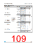
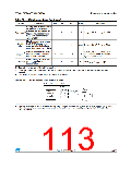
Table 70. DAC characteristics (continued)
Symbol
Parameter
Min
Typ
Max
Unit
Settling time (full scale: for a
10-bit input code transition
(3) between the lowest and the
highest input codes when
DAC_OUT reaches final
value 1LSB
tSETTLING
-
3
4
µs CLOAD ≤ 50 pF, RLOAD ≥ 5 kΩ
Max frequency for a correct
Update DAC_OUT change when
-
-
1
MS/s CLOAD ≤ 50 pF, RLOAD ≥ 5 kΩ
CLOAD ≤ 50 pF, RLOAD ≥ 5 kΩ
rate(3)
small variation in the input
code (from code i to i+1LSB)
Wakeup time from off state
(Setting the ENx bit in the
DAC Control register)
(3)
tWAKEUP
-
-
6.5
10
µs
input code between lowest and
highest possible ones.
Power supply rejection ratio
PSRR+ (1) (to VDDA) (static DC
measurement
–67
–40
dB No RLOAD, CLOAD = 50 pF
1. Guaranteed by design, not tested in production.
2. Quiescent mode refers to the state of the DAC a keeping steady value on the output, so no dynamic consumption is
involved.
3. Data based on characterization results, not tested in production.
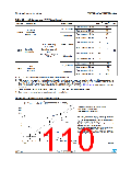
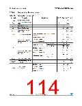
Figure 34. 12-bit buffered /non-buffered DAC
Buffered/Non-buffered DAC
Buffer(1)
RLOAD
DACx_OUT
12-bit
digital to
analog
converter
CLOAD
ai17157
1. The DAC integrates an output buffer that can be used to reduce the output impedance and to drive external loads directly
without the use of an external operational amplifier. The buffer can be bypassed by configuring the BOFFx bit in the
DAC_CR register.
Doc ID 023353 Rev 5
113/133

 STMICROELECTRONICS [ ST ]