Electrical characteristics
STM32F302xx/STM32F303xx
6.3.19
DAC electrical specifications
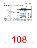
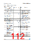
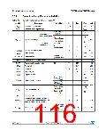
Table 70. DAC characteristics
Symbol
Parameter
Min
Typ
Max
Unit
Comments
Analog supply voltage for
DAC ON
VDDA
2.4
5
-
-
3.6
-
V
(1)
RLOAD
Resistive load with buffer ON
kΩ
When the buffer is OFF, the Minimum
resistive load between DAC_OUT
and VSS to have a 1% accuracy is
1.5 MΩ
Impedance output with buffer
OFF
(1)
RO
-
-
15
kΩ
Maximum capacitive load at
pF DAC_OUT pin (when the buffer is
ON).
(1)
CLOAD
Capacitive load
-
-
-
50
-
It gives the maximum output
excursion of the DAC.
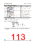
DAC_OUT Lower DAC_OUT voltage
min(1)
with buffer ON
0.2
V
It corresponds to 12-bit input code
(0x0E0) to (0xF1C) at VDDA = 3.6 V
DAC_OUT Higher DAC_OUT voltage
max(1) with buffer ON
and (0x155) and (0xEAB) at VDDA
2.4 V
=
-
-
-
-
-
-
VDDA – 0.2
V
mV
V
DAC_OUT Lower DAC_OUT voltage
0.5
-
VDDA – 1LSB
380
min(1)
with buffer OFF
It gives the maximum output
excursion of the DAC.
DAC_OUT Higher DAC_OUT voltage
max(1) with buffer OFF
-
-
-
With no load, middle code (0x800) on
the input
µA
µA
DAC DC current
(3)
IDDA
consumption in quiescent
mode (Standby mode)(2)
With no load, worst code (0xF1C) on
the input
480
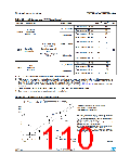
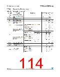
Differential non linearity
-
-
0.5
LSB Given for a 10-bit input code
DNL(3) Difference between two
consecutive code-1LSB)
-
-
-
-
2
1
LSB Given for a 12-bit input code
LSB Given for a 10-bit input code
Integral non linearity
(difference between
measured value at Code i
and the value at Code i on a
INL(3)
-
-
4
LSB Given for a 12-bit input code
mV
line drawn between Code 0
and last Code 1023)
-
-
-
-
10
3
Offset error
Given for a 10-bit input code at VDDA
(difference between
measured value at Code
LSB
Offset(3)
= 3.6 V
(0x800) and the ideal value =
VDDA/2)
Given for a 12-bit input code at VDDA
= 3.6 V
-
-
-
-
12
LSB
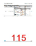
Gain
Gain error
error(3)
0.5
% Given for a 12-bit input code
112/133
Doc ID 023353 Rev 5

 STMICROELECTRONICS [ ST ]