STM32F103x8, STM32F103xB
Electrical characteristics
5.3.4
Embedded reference voltage
The parameters given in Table 12 are derived from tests performed under ambient
temperature and V supply voltage conditions summarized in Table 9.
DD
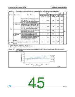
Table 12. Embedded internal reference voltage
Symbol
Parameter
Conditions
Min
Max
Unit
Typ
–40 °C < TA < +105 °C 1.16 1.20
1.26
1.24
V
V
VREFINT Internal reference voltage
–40 °C < TA < +85 °C
1.16 1.20
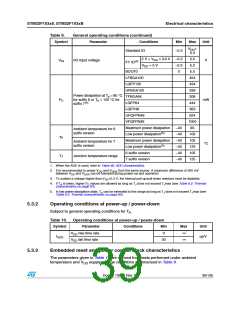
5.1
ADC sampling time when
reading the internal reference
voltage
(1)
17.1(2)
10
TS_vrefint
µs
Internal reference voltage
spread over the temperature
range
(2)
VRERINT
VDD = 3 V 10 mV
mV
(2)
TCoeff
Temperature coefficient
100 ppm/°C
1. Shortest sampling time can be determined in the application by multiple iterations.
2. Guaranteed by design, not tested in production.
5.3.5
Supply current characteristics
The current consumption is a function of several parameters and factors such as the
operating voltage, ambient temperature, I/O pin loading, device software configuration,
operating frequencies, I/O pin switching rate, program location in memory and executed
binary code.
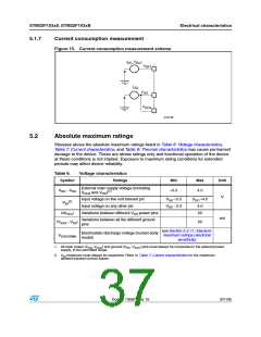
The current consumption is measured as described in Figure 15: Current consumption
measurement scheme.
All Run-mode current consumption measurements given in this section are performed with a
reduced code that gives a consumption equivalent to Dhrystone 2.1 code.
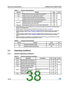
Maximum current consumption
The MCU is placed under the following conditions:
●
●
●
All I/O pins are in input mode with a static value at V or V (no load)
DD SS
All peripherals are disabled except when explicitly mentioned
The Flash memory access time is adjusted to the f frequency (0 wait state from 0
HCLK
to 24 MHz, 1 wait state from 24 to 48 MHz and 2 wait states above)
●
●
Prefetch in ON (reminder: this bit must be set before clock setting and bus prescaling)
When the peripherals are enabled f
= f
/2, f
= f
PCLK1
HCLK
PCLK2 HCLK
The parameters given in Table 13, Table 14 and Table 15 are derived from tests performed
under ambient temperature and V supply voltage conditions summarized in Table 9.
DD
Doc ID 13587 Rev 15
41/105

 STMICROELECTRONICS [ ST ]