STD25NE03L
ELECTRICAL CHARACTERISTICS
(continued)
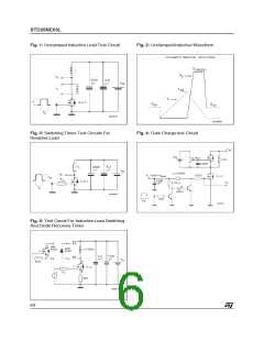
SWITCHING ON
Symbol
Parameter
Test Conditions
Min.
Min.
Min.
Typ.
Max.
Unit
td(on)
tr
Turn-on Delay Time
Rise Time
VDD = 15 V
RG = 4.7
ID = 19 A
VGS = 4.5 V
28
220
ns
ns
Ω
(Resistive Load, see fig. 3)
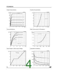
Qg
Qgs
Qgd
Total Gate Charge
Gate-Source Charge
Gate-Drain Charge
VDD = 24 V ID = 38 A VGS = 5 V
21
9
11
29
nC
nC
nC
SWITCHING OFF
Symbol
Parameter
Test Conditions
Typ.
Max.
Unit
td(off)
tf
Turn-off Delay Time
Fall Time
VDD = 15 V
RG = 4.7 Ω
ID = 19 A
VGS = 4.5 V
45
35
ns
ns
(Resistive Load, see fig. 3)
tr(Voff)
tf
tc
Off-voltage Rise Time
Fall Time
Cross-over Time
VDD = 24 V
RG = 4.7 Ω
ID = 38 A
VGS = 4.5 V
30
85
125
ns
ns
ns
(Inductive Load, see fig. 5)
SOURCE DRAIN DIODE
Symbol
Parameter
Test Conditions
Typ.
Max.
Unit
ISD
ISDM ( )
Source-drain Current
Source-drain Current
(pulsed)
20
100
A
A
•
VSD ( ) Forward On Voltage
ISD = 25 A VGS = 0
1.5
V
trr
Reverse Recovery
Time
Reverse Recovery
Charge
Reverse Recovery
Current
ISD = 38 A
VDD = 15 V
(see test circuit, fig. 5)
di/dt = 100 A/ s
45
60
ns
µ
Tj = 150 oC
Qrr
nC
A
IRRM
2.5
( ) Pulsed: Pulse duration = 300 µs, duty cycle 1.5 %
( ) Pulse width limited by safe operating area
•
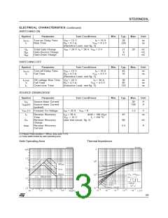
Safe Operating Area
Thermal Impedance
3/9

 STMICROELECTRONICS [ ST ]