ST92F124/F150/F250 - INTERRUPTS
5.1.1.4 Top Level Interrupt (TLI)
5 INTERRUPTS
5.1 INTRODUCTION
In addition, a dedicated interrupt channel, set to
the Top-level priority, can be devoted either to the
external NMI pin (where available) to provide a
Non-Maskable Interrupt, or to the Timer/Watch-
dog. Interrupt service routines are addressed
through a vector table mapped in Memory.
The ST9 responds to peripheral and external
events through its interrupt channels. Current pro-
gram execution can be suspended to allow the
ST9 to execute a specific response routine when
such an event occurs, providing that interrupts
have been enabled, and according to a priority
mechanism. If an event generates a valid interrupt
request, the current program status is saved and
control passes to the appropriate Interrupt Service
Routine.
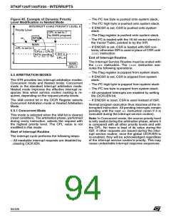
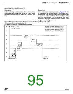
Figure 44. Interrupt Response
n
NORMAL
PROGRAM
FLOW
INTERRUPT
SERVICE
ROUTINE
The ST9 CPU can receive requests from the fol-
lowing sources:
– On-chip peripherals
– External pins
– Top-Level Pseudo-non-maskable interrupt
5.1.1 On-Chip Peripheral Interrupt Sources
5.1.1.1 Dedicated Channels
CLEAR
PENDING BIT
INTERRUPT
The following on-chip peripherals have dedicated
interrupt channels with interrupt control registers
located in their peripheral register page.
IRET
INSTRUCTION
– A/D Converter
2
– I C
VR001833
– JPBLD
– MFT
5.2 INTERRUPT VECTORING
– SCI-M
5.1.1.2 Standard Channels
The ST9 implements an interrupt vectoring struc-
ture which allows the on-chip peripheral to identify
the location of the first instruction of the Interrupt
Service Routine automatically.
Other on-chip peripherals have their interrupts
mapped to the INTxx interrupt channel group.
These channels have control registers located in
Pages 0 and 60. These peripherals are:
When an interrupt request is acknowledged, the
peripheral interrupt module provides, through its
Interrupt Vector Register (IVR), a vector to point
into the vector table of locations containing the
start addresses of the Interrupt Service Routines
(defined by the programmer).
– CAN
3 TM
– E
/FLASH
– EFT Timer
– RCCU
Each peripheral has a specific IVR mapped within
its Register File pages (or in register page 0 or 60
if it is mapped to one of the INTxx channels).
– SCI-A
– SPI
– STIM timer
– WDT Timer
– WUIMU
The Interrupt Vector table, containing the address-
es of the Interrupt Service Routines, is located in
the first 256 locations of Memory pointed to by the
ISR register, thus allowing 8-bit vector addressing.
For a description of the ISR register refer to the
chapter describing the MMU.
5.1.1.3 External Interrupts
Up to eight external interrupts, with programmable
input trigger edge, are available and are mapped
to the INTxx interrupt channel group in page 0.
The user Power on Reset vector is stored in the
first two physical bytes in memory, 000000h and
000001h.
91/426
9

 STMICROELECTRONICS [ ST ]