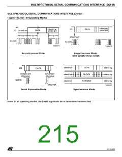
MULTIPROTOCOL SERIAL COMMUNICATIONS INTERFACE (SCI-M)
MULTIPROTOCOL SERIAL COMMUNICATIONS INTERFACE (Cont’d)
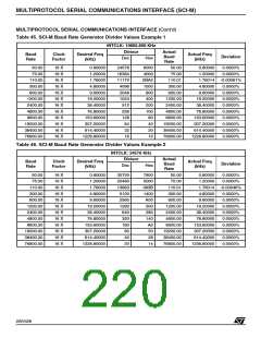
10.5.6 Clocks And Serial Transmission Rates
The output of the Baud Rate generator has a pre-
cise 50% duty cycle. The Baud Rate generator can
use INTCLK for the input clock source. In this
case, INTCLK (and therefore the MCU Xtal)
should be chosen to provide a suitable frequency
for division by the Baud Rate Generator to give the
required transmit and receive bit rates. Suitable
INTCLK frequencies and the respective divider
values for standard Baud rates are shown in Table
45.
The communication bit rate of the SCI transmitter
and receiver sections can be provided from the in-
ternal Baud Rate Generator or from external
sources. The bit rate clock is divided by 16 in
Asynchronous mode (CD in CCR reset), or undi-
vided in the 3 other modes (CD set).
With INTCLK running at 24MHz and no external
Clock provided, a maximum bit rate of 3MBaud
and 750KBaud is available in undivided and divide
by-16-mode respectively.
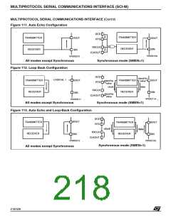
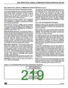
10.5.7 SCI -M Initialization Procedure
Writing to either of the two Baud Rate Generator
Registers immediately disables and resets the SCI
baud rate generator, as well as the transmitter and
receiver circuitry.
With INTCLK running at 24MHz and an external
Clock provided through the RXCLK/TXCLK lines,
a maximum bit rate of 3MBaud and 375KBaud is
available in undivided and divided by 16 mode re-
spectively (see Figure 115).
After writing to the second Baud Rate Generator
Register, the transmitter and receiver circuits are
enabled. The Baud Rate Generator will load the
new value and start counting.
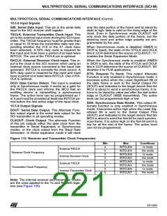
External Clock Sources. The External Clock in-
put pin TXCLK may be programmed by the XTCLK
and OCLK bits in the CCR register as: the transmit
clock input, Baud Rate Generator output (allowing
an external divider circuit to provide the receive
clock for split rate transmit and receive), or as
CLKOUT output in Synchronous and Serial Ex-
pansion modes. The RXCLK Receive clock input
is enabled by the XRX bit, this input should be set
in accordance with the setting of the CD bit.
To initialize the SCI, the user should first initialize
the most significant byte of the Baud Rate Gener-
ator Register; this will reset all SCI circuitry. The
user should then initialize all other SCI registers
(SICR/SOCR included) for the desired operating
mode and then, to enable the SCI, he should ini-
tialize the least significant byte Baud Rate Gener-
ator Register.
Baud Rate Generator. The internal Baud Rate
Generator consists of a 16-bit programmable di-
vide by “N” counter which can be used to generate
the transmitter and/or receiver clocks. The mini-
mum baud rate divisor is 2 and the maximum divi-
'On-the-Fly' modifications of the control registers'
content during transmitter/receiver operations, al-
though possible, can corrupt data and produce un-
desirable spikes on the I/O lines (data, clock and
control). Furthermore, modifying the control regis-
ters' content without reinitialising the SCI circuitry
(during stand-by cycles, waiting to transmit or re-
ceive data) must be kept carefully under control by
software to avoid spurious data being transmitted
or received.
16
sor is 2 -1. After initialising the baud rate genera-
tor, the divisor value is immediately loaded into the
counter. This prevents potentially long random
counts on the initial load.
The Baud Rate generator frequency is equal to the
Input Clock frequency divided by the Divisor value.
WARNING: Programming the baud rate divider to
0 or 1 will stop the divider.
Note: For synchronous receive operation, the data
and receive clock must not exhibit significant skew
between clock and data. The received data and
clock are internally synchronized to INTCLK.
Figure 114. SCI-M Baud Rate Generator Initialization Sequence
MOST SIGNIFICANT
BYTE INITIALIZATION
SELECT SCI
WORKING MODE
LEAST SIGNIFICANT
BYTE INITIALIZATION
219/426
9

 STMICROELECTRONICS [ ST ]