ST6208C/ST6209C/ST6210C/ST6220C
EMC CHARACTERISTICS (Cont’d)
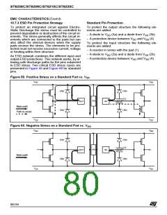
10.7.3 ESD Pin Protection Strategy
Standard Pin Protection
To protect an integrated circuit against Electro-
Static Discharge the stress must be controlled to
prevent degradation or destruction of the circuit el-
ements. The stress generally affects the circuit el-
ements which are connected to the pads but can
also affect the internal devices when the supply
pads receive the stress. The elements to be pro-
tected must not receive excessive current, voltage
or heating within their structure.
To protect the output structure the following ele-
ments are added:
– A diode to V (3a) and a diode from V (3b)
DD
SS
– A protection device between V and V (4)
DD
SS
To protect the input structure the following ele-
ments are added:
– A resistor in series with the pad (1)
– A diode to V (2a) and a diode from V (2b)
DD
SS
An ESD network combines the different input and
output ESD protections. This network works, by al-
lowing safe discharge paths for the pins subjected
to ESD stress. Two critical ESD stress cases are
presented in Figure 59 and Figure 60 for standard
pins.
– A protection device between V and V (4)
DD
SS
Figure 59. Positive Stress on a Standard Pad vs. V
SS
V
V
DD
DD
(3a)
(3b)
(2a)
(1)
(4)
OUT
IN
Main path
(2b)
Path to avoid
V
V
V
SS
SS
Figure 60. Negative Stress on a Standard Pad vs. V
DD
V
DD
DD
(3a)
(3b)
(2a)
(1)
(4)
OUT
IN
Main path
(2b)
V
V
SS
SS
80/104
1

 STMICROELECTRONICS [ ST ]