ST6208C/ST6209C/ST6210C/ST6220C
10.5 CLOCK AND TIMING CHARACTERISTICS
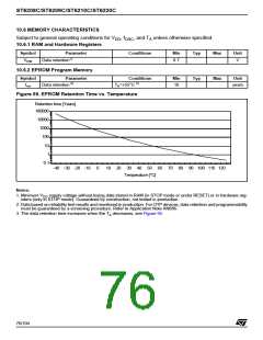
Subject to general operating conditions for V , f
, and T .
DD OSC
A
10.5.1 General Timings
1)
Symbol
Parameter
Conditions
Min
2
Typ
Max
5
Unit
tCPU
µs
4
t
Instruction cycle time
c(INST)
f
f
=8 MHz
3.25
6
6.5
8.125
11
CPU
2)
tCPU
µs
Interrupt reaction time
t
v(IT)
t
= ∆t
+ 6
=8 MHz
9.75
17.875
v(IT)
c(INST)
CPU
10.5.2 External Clock Source
Symbol
Parameter
OSC input pin high level voltage
Conditions
See Figure 49
≤V ≤V
Min
Typ
Max
Unit
V
V
0.7xV
V
DD
OSCINH
IN
DD
V
OSC input pin low level voltage
V
0.3xV
± 2
OSCINL
IN
SS
DD
I
OSCx Input leakage current
V
µA
L
SS
IN
DD
Notes:
1. Data based on typical application software.
2. Time measured between interrupt event and interrupt vector fetch. ∆tc(INST) is the number of tCPU cycles needed to finish
the current instruction execution.
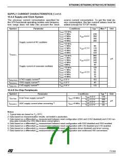
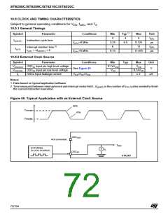
Figure 49. Typical Application with an External Clock Source
90%
V
V
OSCINH
10%
OSCINL
OSC
OUT
Not connected
f
OSC
EXTERNAL
CLOCK SOURCE
I
L
OSC
IN
ST62XX
72/104
1

 STMICROELECTRONICS [ ST ]