ST6208C/ST6209C/ST6210C/ST6220C
I/O PORTS (Cont’d)
7.5 REGISTER DESCRIPTION
DATA REGISTER (DR)
Bits 7:0 = DD[7:0] Data direction register bits.
The DDR register gives the input/output direction
configuration of the pins. Each bit is set and
cleared by software.
Port x Data Register
DRx with x = A or B.
0: Input mode
1: Output mode
Address DRA: 0C0h - Read/Write
Address DRB: 0C1h - Read/Write
Reset Value: 0000 0000 (00h)
OPTION REGISTER (OR)
7
0
Port x Option Register
ORx with x = A or B.
D7
D6
D5
D4
D3
D2
D1
D0
Address ORA: 0CCh - Read/Write
Address ORB: 0CDh - Read/Write
Reset Value: 0000 0000 (00h)
Bits 7:0 = D[7:0] Data register bits.
Reading the DR register returns either the DR reg-
ister latch content (pin configured as output) or the
digital value applied to the I/O pin (pin configured
as input).
7
0
O7
O6
O5
O4
O3
O2
O1
O0
Caution: In input mode, modifying this register will
modify the I/O port configuration (see Table 9).
Bits 7:0 = O[7:0] Option register bits.
Do not use the Single bit instructions on I/O port
data registers. See (Section 7.2.5).
The OR register allows to distinguish in output
mode if the push-pull or open drain configuration is
selected.
Output mode:
DATA DIRECTION REGISTER (DDR)
0: Open drain output(with P-Buffer deactivated)
1: Push-pull Output
Port x Data Direction Register
DDRx with x = A or B.
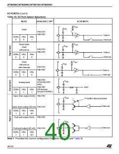
Input mode: See Table 9.
Address DDRA: 0C4h - Read/Write
Address DDRB: 0C5h - Read/Write
Each bit is set and cleared by software.
Caution: Modifying this register, will also modify
the I/O port configuration in input mode. (see Ta-
ble 9).
Reset Value: 0000 0000 (00h)
7
0
DD7
DD6
DD5
DD4
DD3
DD2
DD1
DD0
Table 11. I/O Port Register Map and Reset Values
Address
(Hex.)
Register
Label
7
6
5
4
3
2
1
0
Reset Value
of all I/O port registers
0
0
0
0
0
0
0
0
0C0h
0C1h
0C4h
0C5h
0CCh
0CDh
DRA
MSB
LSB
DRB
DDRA
DDRB
ORA
ORB
MSB
MSB
LSB
LSB
41/104
1

 STMICROELECTRONICS [ ST ]