ST6208C/ST6209C/ST6210C/ST6220C
7 I/O PORTS
7.1 INTRODUCTION
Each I/O port contains up to 8 pins. Each pin can
be programmed independently as digital input
(with or without pull-up and interrupt generation),
digital output (open drain, push-pull) or analog in-
put (when available).
All input lines can be individually connected by
software to the interrupt system by programming
the OR and DR registers accordingly. The inter-
rupt trigger modes (falling edge, rising edge and
low level) can be configured by software for each
port as described in the Interrupt section.
The I/O pins can be used in either standard or al-
ternate function mode.
7.2.2 Analog Inputs
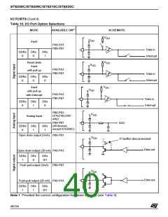
Standard I/O mode is used for:
Some pins can be configured as analog inputs by
programming the OR and DR registers according-
ly, see Table 9. These analog inputs are connect-
ed to the on-chip 8-bit Analog to Digital Converter.
– Transfer of data through digital inputs and out-
puts (on specific pins):
– External interrupt generation
Caution: ONLY ONE pin should be programmed
as an analog input at any time, since by selecting
more than one input simultaneously their pins will
be effectively shorted.
Alternate function mode is used for:
– Alternate signal input/output for the on-chip
peripherals
7.2.3 Output Modes
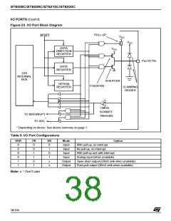
The generic I/O block diagram is shown in Figure
23.
The output configuration is selected by setting the
corresponding DDR register bit. In this case, writ-
ing to the DR register applies this digital value to
the I/O pin through the latch. Then, reading the DR
register returns the previously stored value.
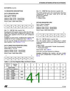
7.2 FUNCTIONAL DESCRIPTION
Each port is associated with 3 registers located in
Data space:
Two different output modes can be selected by
software through the OR register: push-pull and
open-drain.
– Data Register (DR)
– Data Direction Register (DDR)
– Option Register (OR)
DR register value and output pin status:
Each I/O pin may be programmed using the corre-
sponding register bits in the DDR, DR and OR reg-
isters: bit x corresponding to pin x of the port. Table
9 illustrates the various port configurations which
can be selected by user software.
DR
0
Push-pull
Open-drain
V
V
V
SS
SS
DD
1
Floating
Note: The open drain setting is not a true open
drain. This means it has the same structure as the
push-pull setting but the P-buffer is deactivated.
To avoid damaging the device, please respect the
During MCU initialization, all I/O registers are
cleared and the input mode with pull-up and no in-
terrupt generation is selected for all the pins, thus
avoiding pin conflicts.
V
absolute maximum rating described in the
Electrical Characteristics section.
OUT
7.2.1 Digital Input Modes
7.2.4 Alternate Functions
The input configuration is selected by clearing the
corresponding DDR register bit.
When an on-chip peripheral is configured to use a
pin, the alternate function (timer input/output...) is
not systematically selected but has to be config-
ured through the DDR, OR and DR registers. Re-
fer to the chapter describing the peripheral for
more details.
In this case, reading the DR register returns the
digital value applied to the external I/O pin.
Different input modes can be selected by software
through the DR and OR registers, see Table 9.
External Interrupt Function
37/104
1

 STMICROELECTRONICS [ ST ]