ST10F276E
Electrical characteristics
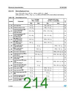
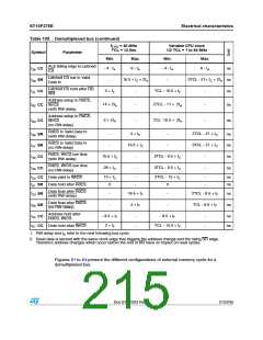
Table 105. Demultiplexed bus (continued)
fCPU = 40 MHz
TCL = 12.5ns
Variable CPU clock
1/2 TCL = 1 to 64 MHz
Symbol
Parameter
Min.
Max.
Min.
Max.
ALE falling edge to Latched
CS
- 4 - tA
6 - tA
- 4 - tA
6 - tA
t38 CC
t39 SR
t41 CC
ns
ns
ns
Latched CS low to Valid
Data In
16.5 + tC + 2tA
3TCL - 21+ tC + 2tA
-
-
Latched CS hold after RD,
WR
2 + tF
TCL - 10.5 + tF
-
-
Address setup to RdCS,
t82 CC WrCS
(with RW-delay)
14 + 2tA
2 + 2tA
2TCL - 11 + 2tA
TCL -10.5 + 2tA
-
-
-
-
ns
ns
Address setup to RdCS,
t83 CC WrCS
(no RW-delay)
RdCS to Valid Data In
(with RW-delay)
4 + tC
2TCL - 21 + tC
t46 SR
t47 SR
t48 CC
t49 CC
-
-
ns
ns
ns
ns
RdCS to Valid Data In
(no RW-delay)
16.5 + tC
3TCL - 21 + tC
-
-
RdCS, WrCS low time
(with RW-delay)
15.5 + tC
28 + tC
2TCL - 9.5 + tC
3TCL - 9.5 + tC
-
-
-
-
RdCS, WrCS low time
(no RW-delay)
10 + tC
0
2TCL - 15 + tC
0
t50 CC Data valid to WrCS
t51 SR Data hold after RdCS
-
-
-
-
ns
ns
Data float after RdCS
t53 SR
16.5 + tF
4 + tF
2TCL - 8.5 + tF
TCL - 8.5 + tF
-
-
-
-
ns
ns
(with RW-delay)
Data float after RdCS
t68 SR
(no RW-delay)
Address hold after
t55 CC
- 8.5 + tF
2 + tF
- 8.5 + tF
-
-
-
-
ns
ns
RdCS, WrCS
TCL - 10.5 + tF
t57 CC Data hold after WrCS
1. RW-delay and tA refer to the next following bus cycle.
2. Read data is latched with the same clock edge that triggers the address change and the rising RD edge.
Therefore address changes which occur before the end of RD have no impact on read cycles.
1
Partially tested, guaranteed by design characterization.
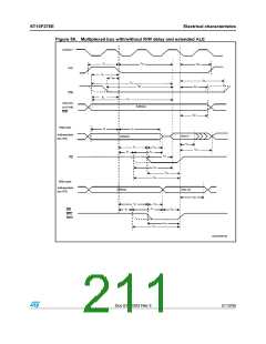
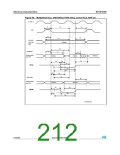
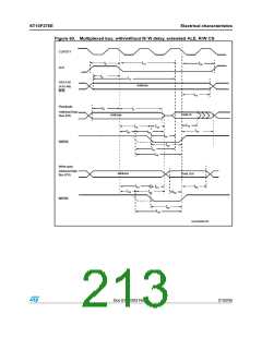
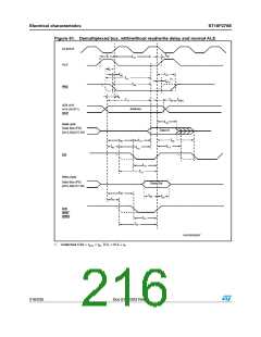
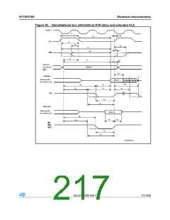
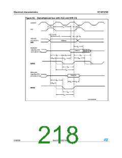
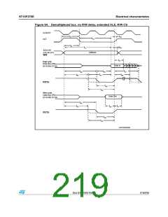
Figures 61 to 64 present the different configurations of external memory cycle for a
demultiplexed bus.
Doc ID 12303 Rev 3
215/235

 STMICROELECTRONICS [ ST ]