ST10F276E
System reset
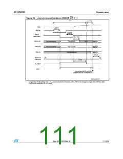
19.2
Asynchronous reset
An asynchronous reset is triggered when RSTIN pin is pulled low while RPD pin is at low
level. Then the ST10F276E is immediately (after the input filter delay) forced in reset default
state. It pulls low RSTOUT pin, it cancels pending internal hold states if any, it aborts all
internal/external bus cycles, it switches buses (data, address and control signals) and I/O
pin drivers to high-impedance, it pulls high Port0 pins.
Note:
If an asynchronous reset occurs during a read or write phase in internal memories, the
content of the memory itself could be corrupted: to avoid this, synchronous reset usage is
strongly recommended.
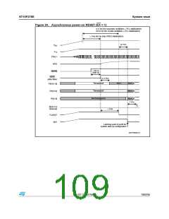
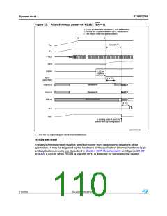
Power-on reset
The asynchronous reset must be used during the power-on of the device. Depending
on crystal or resonator frequency, the on-chip oscillator needs about 1ms to 10ms to
stabilize (refer to Chapter 23: Electrical characteristics), with an already stable VDD. The
logic of the ST10F276E does not need a stabilized clock signal to detect an asynchronous
reset, so it is suitable for power-on conditions. To ensure a proper reset sequence, the
RSTIN pin and the RPD pin must be held at low level until the device clock signal is
stabilized and the system configuration value on Port0 is settled.
At Power-on it is important to respect some additional constraints introduced by the start-up
phase of the different embedded modules.
In particular the on-chip voltage regulator needs at least 1ms to stabilize the internal 1.8V
for the core logic: this time is computed from when the external reference (VDD) becomes
stable (inside specification range, that is at least 4.5V). This is a constraint for the
application hardware (external voltage regulator): the RSTIN pin assertion shall be extended
to guarantee the voltage regulator stabilization.
A second constraint is imposed by the embedded Flash. When booting from internal
memory, starting from RSTIN releasing, it needs a maximum of 1ms for its initialization:
before that, the internal reset (RST signal) is not released, so the CPU does not start code
execution in internal memory.
Note:
This is not true if external memory is used (pin EA held low during reset phase). In this case,
once RSTIN pin is released, and after few CPU clock (Filter delay plus 3...8 TCL), the
internal reset signal RST is released as well, so the code execution can start immediately
after. Obviously, an eventual access to the data in internal Flash is forbidden before its
initialization phase is completed: an eventual access during starting phase will return FFFFh
(just at the beginning), while later 009Bh (an illegal opcode trap can be generated).
At Power-on, the RSTIN pin shall be tied low for a minimum time that includes also the start-
up time of the main oscillator (tSTUP = 1ms for resonator, 10ms for crystal) and PLL
synchronization time (tPSUP = 200μs): this means that if the internal Flash is used, the
RSTIN pin could be released before the main oscillator and PLL are stable to recover some
time in the start-up phase (Flash initialization only needs stable V18, but does not need
stable system clock since an internal dedicated oscillator is used).
Warning: It is recommended to provide the external hardware with a
current limitation circuitry. This is necessary to avoid
permanent damages of the device during the power-on
transient, when the capacitance on V18 pin is charged. For
the on-chip voltage regulator functionality 10nF are
Doc ID 12303 Rev 3
107/235

 STMICROELECTRONICS [ ST ]