M29F400BT, M29F400BB
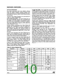
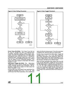
Figure 4. Data Polling Flowchart
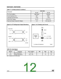
Figure 5. Data Toggle Flowchart
START
START
READ
READ DQ5 & DQ7
at VALID ADDRESS
DQ5 & DQ6
READ DQ6
DQ7
=
DATA
YES
DQ6
=
NO
NO
TOGGLE
YES
NO
DQ5
= 1
NO
DQ5
= 1
YES
YES
READ DQ7
at VALID ADDRESS
READ DQ6
TWICE
DQ7
=
DATA
YES
DQ6
=
NO
TOGGLE
NO
FAIL
YES
PASS
FAIL
PASS
AI01370B
AI03598
Erase Timer Bit (DQ3). The Erase Timer Bit can
be used to identify the start of Program/Erase
Controller operation during a Block Erase com-
mand. Once the Program/Erase Controller starts
erasing the Erase Timer Bit is set to ’1’. Before the
Program/Erase Controller starts the Erase Timer
Bit is set to ’0’ and additional blocks to be erased
may be written to the Command Interface. The
Erase Timer Bit is output on DQ3 when the Status
Register is read.
Alternative Toggle Bit (DQ2). The Alternative
Toggle Bit can be used to monitor the Program/
Erase controller during Erase operations. The Al-
ternative Toggle Bit is output on DQ2 when the
Status Register is read.
within the blocks being erased. Once the operation
completes the memory returns to Read mode.
During Erase Suspend the Alternative Toggle Bit
changes from ’0’ to ’1’ to ’0’, etc. with successive
Bus Read operations from addresses within the
blocks being erased. Bus Read operations to ad-
dresses within blocks not being erased will output
the memory cell data as if in Read mode.
After an Erase operation that causes the Error Bit
to be set the Alternative Toggle Bit can be used to
identify which block or blocks have caused the er-
ror. The Alternative Toggle Bit changes from ’0’ to
’1’ to ’0’, etc. with successive Bus Read Opera-
tions from addresses within blocks that have not
erased correctly. The Alternative Toggle Bit does
not change if the addressed block has erased cor-
rectly.
During Chip Erase and Block Erase operations the
Toggle Bit changes from ’0’ to ’1’ to ’0’, etc., with
successive Bus Read operations from addresses
11/22

 STMICROELECTRONICS [ ST ]