LM158,A-LM258,A-LM358,A
LM158A-LM258A
LM358A
LM158-LM258
LM358
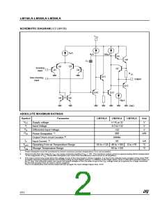
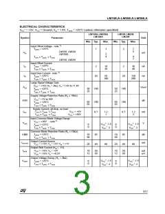
Symbol
Parameter
Unit
Min. Typ.
Max.
Min. Typ.
Max.
+
High Level Output Voltage (V
= 30V)
CC
T
T
= +25°C
R = 2kΩ
L
amb
26
26
27
27
27
28
26
26
27
27
27
28
V
V
≤ T
≤ T
amb
OH
min
max
T
= +25°C
R = 10kΩ
L
amb
T
≤ T
≤ T
amb
min
max
Low Level Output Voltage (R = 10kΩ)
L
V
T
T
= +25°C
5
20
20
5
20
20
mV
V/µs
MHz
%
OL
amb
≤ T
≤ T
amb max
min
Slew Rate
= 15V, V = 0.5 to 3V, R = 2kΩ,
V
SR
CC
i
L
C = 100pF, unity Gain
0.3
0.7
0.6
0.3
0.7
0.6
L
Gain Bandwidth Product
V
= 30V, f =100kHz,V = 10mV, R = 2kΩ,
GBP
THD
CC
in L
C = 100pF
1.1
1.1
L
Total Harmonic Distortion
f = 1kHz, A = 20dB, R = 2kΩ, V = 2V ,
C = 100pF, V = 2Vpp
v
L
o
pp
0.02
0.02
L
O
nV
Equivalent Input Noise Voltage
-----------
e
n
f = 1kHz, R = 100Ω, V = 30V
55
55
s
CC
Hz
DV
DI
Input Offset Voltage Drift
Input Offset Current Drift
7
15
7
30
µV/°C
pA/°C
io
10
200
10
300
Iio
4)
Channel Separation - note
V
/V
dB
o1 o2
120
120
1kHz ≤ f ≤ 20kHZ
1.
Vo = 1.4V, Rs = 0Ω, 5V < VCC+ < 30V, 0 < Vic < VCC+ - 1.5V
2.
3.
4.
The direction of the input current is out of the IC. This current is essentially constant, independent of the state of the output so no loading change
exists on the input lines.
The input common-mode voltage of either input signal voltage should not be allowed to go negative by more than 0.3V. The upper end of the
common-mode voltage range is VCC+ - 1.5V, but either or both inputs can go to +32V without damage.
Due to the proximity of external components insure that coupling is not originating via stray capacitance between these external parts. This typically
can be detected as this type of capacitance increases at higher frequences.
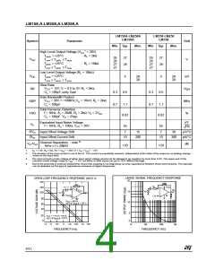
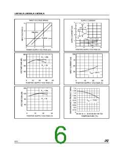
LARGE SIGNAL FREQUENCY RESPONSE
20
(NOTE 3)
OPEN LOOP FREQUENCY RESPONSE
140
100k
W
10M
W
1k
W
0.1 F
m
120
100
+15V
-
V
-
VO
CC
V
15
10
I
V
V
I
O
V
/2
CC
2k
+
W
+7V
+
80
60
40
V
-55°C
= 30V &
CC
T
amb
+125°C
5
0
20
0
V
CC
-55°C
= +10 to + 15V &
T
amb
+125°C
1.0 10 100 1k
10k 100k 1M 10M
1k 10k 100k 1M
FREQUENCY (Hz)
FREQUENCY (Hz)
4/12

 STMICROELECTRONICS [ ST ]