LM158,A-LM258,A-LM358,A
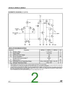
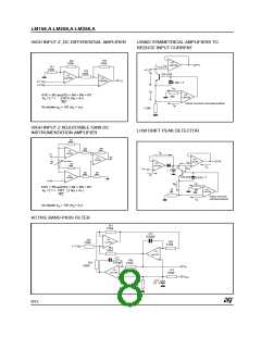
SCHEMATIC DIAGRAM (1/2 LM158)
VCC
6µA
4µA
100µA
Q5
Q6
C C
Q3
Q2
Inverting
input
Q7
Q1
Q4
R SC
Q11
Non-inverting
input
Output
Q13
Q10
Q12
Q8
Q9
50µA
GND
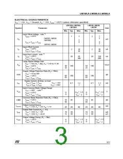
ABSOLUTE MAXIMUM RATINGS
Symbol
Parameter
LM158,A
LM258,A
LM358,A
Unit
V
Supply voltage
Input Voltage
+/-16 or 32
-0.3 to +32
+32
V
V
CC
V
i
V
Differential Input Voltage
V
id
1)
P
500
mW
Power Dissipation
tot
2)
Infinite
50
Output Short-circuit Duration
3)
I
mA
°C
Input Current
in
T
Opearting Free-air Temperature Range
-55 to +125 -40 to +105
0 to +70
oper
T
Storage Temperature Range
-65 to +150
°C
stg
1.
2.
Power dissipation must be considered to ensure maximum junction temperature (Tj) is not exceeded.
Short-circuits from the output to VCC can cause excessive heating if VCC > 15V. The maximum output current is approximately 40mA independent
of the magnitude of VCC. Destructive dissipation can result from simultaneous short-circuit on all amplifiers.
3.
This input current only exists when the voltage at any of the input leads is driven negative. It is due to the collector-base junction of the input PNP
transistor becoming forward biased and thereby acting as input diodes clamps. In addition to this diode action, there is also NPN parasitic action on
the IC chip. this transistor action can cause the output voltages of the Op-amps to go to the VCC voltage level (or to ground for a large overdrive)
for the time duration than an input is driven negative.
This is not destructive and normal output will set up again for input voltage higher than -0.3V.
2/12

 STMICROELECTRONICS [ ST ]