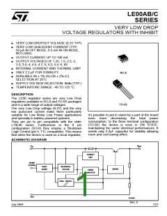
LE00AB/C SERIES
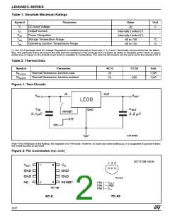
Table 1: Absolute Maximum Ratings
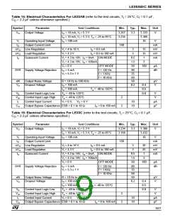
Symbol
Parameter
Value
Unit
V
DC Input Voltage
20
V
I
I
Output Current
Internally Limited (*)
Internally Limited (*)
-40 to 150
O
P
Power Dissipation
tot
T
Storage Temperature Range
Operating Junction Temperature Range
°C
°C
stg
T
-40 to 125
op
(*) Our SO-8 package used for Voltage Regulators is modified internally to have pins 2, 3, 6 and 7 electrically communed to the die attach
flag. This particular frame decreases the total thermal resistance of the package and increases its ability to dissipate power when an appro-
priate area of copper on the printed circuit board is available for heatsinking. The external dimensions are the same as for the standard SO-8.
Table 2: Thermal Data
Symbol
Parameter
SO-8
TO-92
Unit
R
Thermal Resistance Junction-case
Thermal Resistance Junction-ambient
20
55
°C/W
°C/W
thj-case
R
200
thj-amb
Figure 1: Test Circuits
Note: If the Inhibit pin is left floating, the regulator is in ON mode. However, to avoid any noise picking-up, it is suggested to ground it when
the Inhibit function is not used.
Figure 2: Pin Connection (top view)
BOTTOM VIEW
PIN 1 = V
OUT
PIN 2 = GND
PIN 3 = V
IN
SO-8
TO-92
2/27

 STMICROELECTRONICS [ ST ]