LE00AB/C SERIES
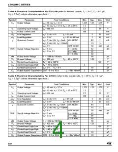
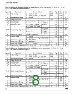
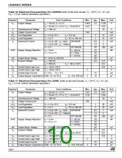
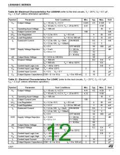
Table 12: Electrical Characteristics For LE30AB (refer to the test circuits, T = 25°C, C = 0.1 µF,
j
I
C = 2.2 µF unless otherwise specified.)
O
Symbol
Parameter
Output Voltage
Test Conditions
= 10 mA, V = 5 V
Min.
2.970
2.940
Typ.
Max.
3.030
3.060
18
Unit
V
I
I
I
3
V
O
O
O
O
I
= 10 mA, V = 5 V, T = -25 to 85°C
I
a
V
Operating Input Voltage
Output Current Limit
Line Regulation
= 100 mA
V
I
I
150
mA
mV
mV
mA
O
∆V
∆V
V = 3.7 to 18 V,
I
I
= 0.5 mA
3
15
15
1
O
O
I
O
Load Regulation
V = 4 V
= 0.5 to 100 mA
ON MODE
3
I
O
I
Quiescent Current
V = 4 to 18V, I = 0mA
0.5
1.5
50
d
I
O
V = 4 to 18V, I = 100mA
3
I
O
V = 6 V
OFF MODE
100
µA
dB
I
SVR Supply Voltage Rejection
I
= 5 mA
V = 5 ± 1 V
f = 120 Hz
f = 1 KHz
f = 10 KHz
81
76
60
50
0.2
O
I
eN
Output Noise Voltage
Dropout Voltage
B = 10 Hz to 100 KHz
µV
V
V
I
I
= 100 mA
= 100 mA
0.4
0.5
0.8
d
O
T = -40 to 125°C
O
a
V
Control Input Logic Low
Control Input Logic High
Control Input Current
T = -40 to 125°C
V
V
IL
a
V
T = -40 to 125°C
2
2
IH
a
I
V = 6 V,
V = 6 V
10
10
µA
µF
I
I
C
C
Output Bypass Capacitance ESR = 0.1 to 10 Ω
I = 0 to 100 mA
O
O
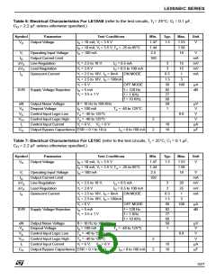
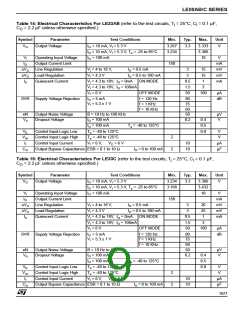
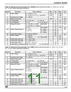
Table 13: Electrical Characteristics For LE30C (refer to the test circuits, T = 25°C, C = 0.1 µF,
j
I
C = 2.2 µF unless otherwise specified.)
O
Symbol
Parameter
Output Voltage
Test Conditions
= 10 mA, V = 5 V
Min.
2.940
2.880
Typ.
Max.
3.060
3.120
18
Unit
V
I
I
I
3
O
O
O
O
I
= 10 mA, V = 5 V, T = -25 to 85°C
I
a
V
Operating Input Voltage
Output Current Limit
Line Regulation
= 100 mA
V
I
I
150
mA
mV
mV
mA
O
∆V
∆V
V = 3.7 to 18 V,
I
I
= 0.5 mA
3
20
25
1
O
O
I
O
Load Regulation
V = 4 V
= 0.5 to 100 mA
ON MODE
3
I
O
I
Quiescent Current
V = 4 to 18V, I = 0mA
0.5
1.5
50
d
I
O
V = 4 to 18V, I = 100mA
3
I
O
V = 6 V
OFF MODE
100
µA
dB
I
SVR Supply Voltage Rejection
I
= 5 mA
V = 5 ± 1 V
f = 120 Hz
f = 1 KHz
f = 10 KHz
81
76
60
50
0.2
O
I
eN
Output Noise Voltage
Dropout Voltage
B = 10 Hz to 100 KHz
µV
V
V
I
I
= 100 mA
= 100 mA
0.4
0.5
0.8
d
O
O
T = -40 to 125°C
a
V
Control Input Logic Low
Control Input Logic High
Control Input Current
T = -40 to 125°C
V
V
IL
a
V
T = -40 to 125°C
2
2
IH
a
I
V = 6 V,
V = 6 V
10
10
µA
µF
I
I
C
C
Output Bypass Capacitance ESR = 0.1 to 10 Ω
I = 0 to 100 mA
O
O
8/27

 STMICROELECTRONICS [ ST ]