L6562A
Application information
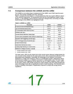
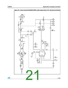
7.5
Comparison between the L6562A and the L6562
The L6562A is not a direct drop-in replacement of the L6562, even if both have the same
pin-out. One function (Disable) has been relocated.
Table 2 compares the two devices, i.e. those parameters that may result in different values
of the external components. The parameters that have the most significant impact on the
design, i.e. that definitely require external component changes when converting an L6562-
based design to the L6562A, are highlighted in bold.
Table 6. L6562A vs. L6562
Parameter
IC turn-on & turn-off thresholds (typ.)
Turn-off threshold spread (max.)
IC consumption before start-up (max.)
Multiplier gain (typ.)
L6562
12/9.5 V
0.8 V
L6562A
12.5/10 V
0.5 V
70 uA
0.6
60 uA
0.38
Current sense reference clamp (typ.)
1.7 V
200 ns
1.08 V
175 ns
Current sense propagation delay (delay-to-output) (typ.)
Dynamic OVP triggering current (typ.)
40 uA
27 uA
ZCD arm/trigger/clamp thresholds (typ.)
Enable threshold (typ.)
2.1/1.4/0.7 V
1.4/0.7/0 V
0.3 V (1)
2.6 V
No
0.45 V (2)
2.2 V
Gate-driver internal drop (max.)
Leading-edge blanking on current sense
Reference voltage accuracy ( overall)
Yes
2.4%
1.8%
1. Function located on pin 5 (ZCD)
2. Function located on pin 1 (INV)
The lower value (-36%) for the clamp level of the current sense reference voltage allows the
use of a lower sense resistor for the same peak current, with a proportional reduction of the
associated power dissipation. Essentially, the advantage is the reduction of the power
dissipated in a single point (hotspot), which is a considerable benefit in applications where
heat removal is critical, e.g. in adapters enclosed in a sealed plastic case. The lower value
for the Dynamic OVP triggering current allows the use of a higher resistance value (+48%)
for the upper resistor of the divider sensing the output voltage of the PFC stage (keeping the
same overvoltage level) with no significant increase of noise sensitivity. This reduction goes
in favor of standby consumption in applications required to comply with energy saving
regulations.
17/26

 STMICROELECTRONICS [ ST ]