L6562A
Application information
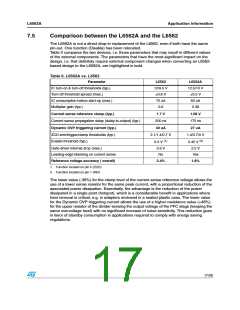
7
Application information
7.1
Overvoltage protection
Under steady-state conditions, the voltage control loop keeps the output voltage Vo of a
PFC pre-regulator close to its nominal value, set by the resistors R1 and R2 of the output
divider. Neglecting ripple components, the current through R1, IR1, equals that through R2,
IR2. Considering that the non-inverting input of the error amplifier is internally referenced at
2.5V, also the voltage at pin INV will be 2.5V, then:
Equation 1
V
O – 2.5
2.5
R2
IR2 = IR1 = ------- = ---------------------
R1
If the output voltage experiences an abrupt change ∆Vo > 0 due to a load drop, the voltage
at pin INV will be kept at 2.5V by the local feedback of the error amplifier, a network
connected between pins INV and COMP that introduces a long time constant to achieve
high PF (this is why ∆Vo can be large). As a result, the current through R2 will remain equal
to 2.5/R2 but that through R1 will become:
Equation 2
V
O – 2.5 + ∆VO
I'R1 = ---------------------------------------
R1
The difference current ∆IR1=I'R1-IR2=I'R1-IR1= ∆Vo/R1 will flow through the compensation
network and enter the error amplifier output (pin COMP). This current is monitored inside
the device and if it reaches about 24µA the output voltage of the multiplier is forced to
decrease, thus smoothly reducing the energy delivered to the output. As the current
exceeds 27µA, the OVP is triggered (Dynamic OVP): the gate-drive is forced low to switch
off the external power transistor and the IC put in an idle state. This condition is maintained
until the current falls below approximately 7µA, which re-enables the internal starter and
allows switching to restart. The output ∆Vo that is able to trigger the Dynamic OVP function
is then:
Equation 3
- 6
∆
V = R1 · 20 · 10
O
An important advantage of this technique is that the OV level can be set independently of
the regulated output voltage: the latter depends on the ratio of R1 to R2, the former on the
individual value of R1. Another advantage is the precision: the tolerance of the detection
current is 13%, i.e. 13% tolerance on ∆Vo. Since ∆Vo << Vo, the tolerance on the absolute
value will be proportionally reduced.
Example: Vo = 400V, ∆Vo = 40V. Then: R1 = 40V/27µA ≈ 1.5MΩ ;
R2 = 1.5 MΩ ·2.5/(400-2.5) = 9.43kΩ. The tolerance on the OVP level due to the L6562A will
be 40·0.13 = 5.3V, that is 1.2%.
13/26

 STMICROELECTRONICS [ ST ]