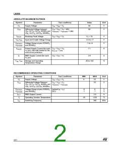
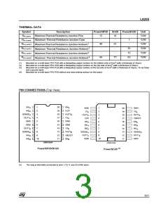
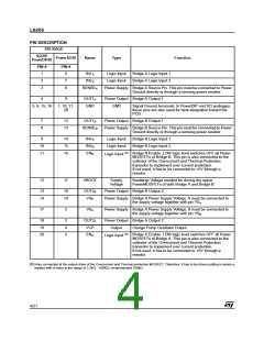
L6205
ELECTRICAL CHARACTERISTICS (continued)
(T
amb
= 25 °C, V = 48V, unless otherwise specified)
s
Symbol
Parameter
Test Conditions
=2.8A, Resistive Load
=2.8A, Resistive Load
Min
Typ
Max
Unit
ns
t
Input to out turn OFF delay time
I
I
600
D(off)IN
LOAD
(8)
t
40
250
ns
FALL
LOAD
Output Fall Time
t
Dead Time Protection
0.5
1
µs
dt
f
-25°C<T <125°C
0.6
1
MHz
CP
j
Charge pump frequency
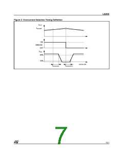
Over Current Protection
(7)
I
Input Supply Overcurrent
Protection Threshold
4
5.6
7.1
60
A
SOVER
T = -25°C to 125°C
j
R
Open Drain ON Resistance
OCD Turn-on Delay Time (9)
OCD Turn-off Delay Time (9)
I = 4mA
40
Ω
OPDR
t
I = 4mA; C < 100pF
200
100
ns
ns
OCD(ON)
EN
t
I = 4mA; C < 100pF
EN
OCD(OFF)
(7)
(8)
(9)
Tested at 25°C in a restricted range and guaranteed by characterization.
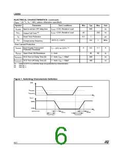
See Fig. 1.
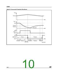
See Fig. 2.
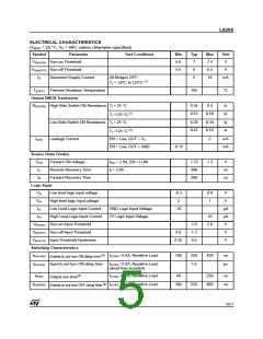
Figure 1. Switching Characteristic Definition
EN
V
th(ON)
V
th(OFF)
t
I
OUT
90%
10%
t
D01IN1316
t
t
RISE
FALL
t
t
D(ON)EN
D(OFF)EN
6/21

 STMICROELECTRONICS [ ST ]