L6205
APPLICATION INFORMATION
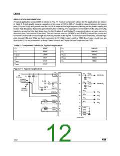
A typical application using L6205 is shown in Fig. 11. Typical component values for the application are shown
in Table 2. A high quality ceramic capacitor in the range of 100 to 200 nF should be placed between the power
pins (VS and VS ) and ground near the L6205 to improve the high frequency filtering on the power supply and
A
B
reduce high frequency transients generated by the switching. The capacitors connected from the EN and EN
A
B
inputs to ground set the shut down time for the Brgidge A and Bridge B respectively when an over current is
detected (see Overcurrent Protection). The two current sources (SENSE and SENSE ) should be connected
A
B
to Power Ground with a trace length as short as possible in the layout. To increase noise immunity, unused logic
pins (except EN and EN ) are best connected to 5V (High Logic Level) or GND (Low Logic Level) (see pin
A
B
description). It is recommended to keep Power Ground and Signal Ground separated on PCB.
Table 2. Component Values for Typical Application
C
C
C
C
C
C
100uF
100nF
220nF
10nF
D
D
R
R
R
1N4148
1N4148
100kΩ
100kΩ
100Ω
1
1
2
2
BOOT
P
ENA
ENB
P
5.6nF
5.6nF
ENA
ENB
Figure 11. Typical Application
VSA
VSB
RENA
CENA
RENB
CENB
ENA
ENB
+
VS
8-52VDC
17
14
20
11
ENABLEA
ENABLEB
C1
C2
POWER
GROUND
-
D1
RP
VCP
19
CP
D2
CBOOT
VBOOT
SENSEA
SENSEB
SIGNAL
GROUND
12
3
IN1B
IN2B
IN1A
IN2A
9
10
1
IN1B
IN2B
IN1A
IN2A
8
LOADA
OUT1A
OUT2A
4
2
18
16
15
6
LOADB
OUT1B
OUT2B
GND
GND
GND
GND
7
13
5
D02IN1345
12/21

 STMICROELECTRONICS [ ST ]