L6205
OUTPUT CURRENT CAPABILITY AND IC POWER DISSIPATION
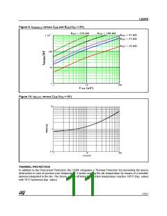
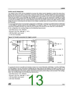
In Fig. 15 and Fig. 16 are shown the approximate relation between the output current and the IC power dissipa-
tion using PWM current control driving two loads, for two different driving types:
– One Full Bridge ON at a time (Fig. 15) in which only one load at a time is energized.
– Two Full Bridges ON at the same time (Fig. 16) in which two loads at the same time are energized.
For a given output current and driving type the power dissipated by the IC can be easily evaluated, in order to
establish which package should be used and how large must be the on-board copper dissipating area to guar-
antee a safe operating junction temperature (125°C maximum).
Figure 15. IC Power Dissipation versus Output Current with One Full Bridge ON at a time.
ONE FULL BRIDGE ON AT A TIME
10
8
IA
IOUT
IB
6
PD [W]
IOUT
4
2
0
Test Conditions:
Supply Voltage = 24V
No PWM
f
SW = 30kHz (slow decay)
0
0.5
1
1.5
2
2.5
3
IOUT [A]
Figure 16. IC Power Dissipation versus Output Current with Two Full Bridges ON at the same time.
TWO FULL BRIDGES ON AT THE SAME TIME
IA
10
IOUT
8
IB
6
IOUT
PD [W]
4
2
0
Test Conditions:
Supply Voltage = 24V
No PWM
fSW = 30kHz (slow decay)
0
0.5
1
1.5
IOUT [A]
2
2.5
3
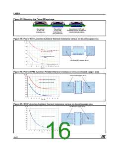
THERMAL MANAGEMENT
In most applications the power dissipation in the IC is the main factor that sets the maximum current that can be de-
liver by the device in a safe operating condition. Therefore, it has to be taken into account very carefully. Besides the
available space on the PCB, the right package should be chosen considering the power dissipation. Heat sinking can
be achieved using copper on the PCB with proper area and thickness. Figures 18, 19 and 20 show the Junction-to-
Ambient Thermal Resistance values for the PowerSO20, PowerDIP20 and SO20 packages.
For instance, using a PowerSO package with copper slug soldered on a 1.5 mm copper thickness FR4 board
2
with 6cm dissipating footprint (copper thickness of 35µm), the R
is about 35°C/W. Fig. 17 shows mount-
th j-amb
ing methods for this package. Using a multi-layer board with vias to a ground plane, thermal impedance can be
reduced down to 15°C/W.
15/21

 STMICROELECTRONICS [ ST ]