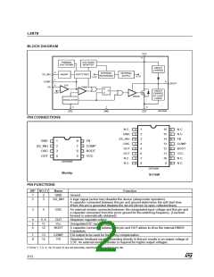
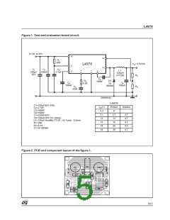
L4978
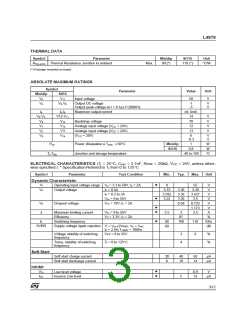
THERMAL DATA
Symbol
Parameter
Minidip
SO16
Unit
Rth(j-amb) Thermal Resistance Junction to ambient
Max.
90 (*)
110 (*)
°C/W
(*) Package mounted on board.
ABSOLUTE MAXIMUM RATINGS
Symbol
Parameter
Value
Unit
Minidip
V5
S016
V11
Input voltage
58
V
V4
V5,V6
Output DC voltage
Output peak voltage at t = 0.1µs f=200KHz
-1
-5
V
V
I4
V6-V5
V6
I5,I6
V12-V11
V12
Maximum output current
int. limit.
14
V
V
V
V
Bootstrap voltage
70
V7
V13
Analogs input voltage (VCC = 24V)
Analogs input voltage (VCC = 24V)
(VCC = 20V)
12
V2
V3
13
V8
V14
6
-0.3
V
V
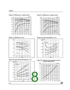
Ptot
Power dissipation a Tamb ≤ 60°C
Minidip
SO16
1
W
W
°C
0.8
Tj,Tstg
Junction and storage temperature
-40 to 150
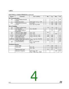
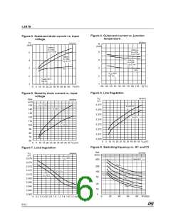
ELECTRICAL CHARACTERISTICS (T = 25°C, Cosc = 2.7nF, Rosc = 20kΩ, VCC = 24V, unless other-
j
wise specified.) * Specification Refered to Tj from 0 to 125°C
Symbol
Parameter
Test Condition
Min.
Typ.
Max.
Unit
Dynamic Characteristic
VI
Operating input voltage range Vo = 3.3 to 50V; Io = 2A
•
•
8
55
V
V
Vo
Output voltage
Io = 0.5A
3.33
3.292
3.22
3.36
3.36
3.36
0.58
3.39
3.427
3.5
Io = 0.2 to 2A
V
V
cc = 8 to 55V
V
Vd
Il
Dropout voltage
Vcc = 10V; Io = 2A
0.733
1.173
3.5
V
•
•
V
Maximum limiting current
Efficiency
Vcc = 8 to 55V
2.5
3
A
Vo = 3.3V; Io = 2A
87
%
KHz
dB
•
fs
Switching frequency
90
60
100
110
6
SVRR
Supply voltage ripple rejection Vi = Vcc+2VRMS; Vo = Vref;
Io = 2.5A; f ripple = 100Hz
Voltage stability of switching
frequency
Vcc = 8 to 55V
3
4
%
%
Temp. stability of switching
frequency
Tj = 0 to 125°C
Soft Start
Soft start charge current
30
6
40
10
50
14
µA
µA
Soft start discharge current
Inhibit
VLL
•
•
Low level voltage
Isource Low level
0.9
15
V
IsLL
5
µA
3/12

 STMICROELECTRONICS [ ST ]