L4978
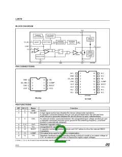
BLOCK DIAGRAM
VCC
5
THERMAL
SHUTDOWN
VOLTAGES
MONITOR
CBOOT
CHARGE
2
INTERNAL
REFERENCE
INTERNAL
SUPPLY
SS_INH
INHIBIT
E/A
SOFTSTART
5.1V
3.3V
7
COMP
6
BOOT
8
FB
PWM
R
Q
S
CBOOT
CHARGE
AT LIGHT
LOADS
3.3V
DRIVE
OSCILLATOR
1
3
4
D97IN594
OSC
GND
OUT
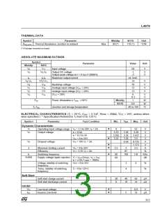
PIN CONNECTIONS
N.C.
GND
1
16
15
14
13
12
11
10
9
N.C.
N.C.
FB
2
3
4
5
6
7
8
SS_INH
OSC
GND
SS_INH
OSC
1
2
3
4
8
7
6
5
FB
COMP
BOOT
VCC
N.C.
N.C.
COMP
BOOT
VCC
OUT
OUT
OUT
N.C.
D97IN595
N.C.
D97IN596
Minidip
SO16W
PIN FUNCTIONS
DIP SO (*)
Name
GND
Function
1
2
2
3
Ground
SS_INH
A logic signal (active low) disables the device (sleep mode operation).
A capacitor connected between this pin and ground determines the soft start time.
When this pin is grounded disables the device (driven by open collector/drain).
3
4
OSC
An external resistor connected between the unregulated input voltage and this pin and
a capacitor connected from this pin to ground fix the switching frequency. (Line feed
forward is automatically obtained)
4
5
6
5, 6
11
OUT
VCC
Stepdown regulator output
Unregulated DC input voltage
12
BOOT
A capacitor connected between this pin and OUT allows to drive the internal DMOS
Transistors
7
8
13
14
COMP
FB
E/A output to be used for frequency compensation
Stepdown feedback input. Connecting directly to this pin results in an output voltage of
3.3V. An external resistive divider is required for higher output voltages.
(*) Pins 1, 7, 8, 9, 10, 15 and 16 are not internally, electrically connected to the die.
2/12

 STMICROELECTRONICS [ ST ]