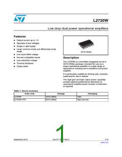
L2720W
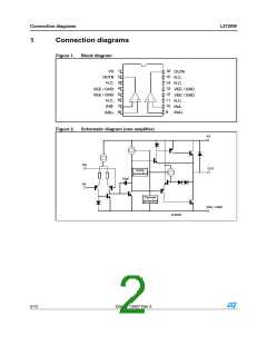
Pin out
2
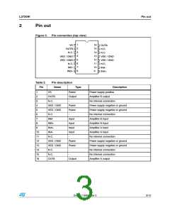
Pin out
Figure 3.
Pin connection (top view)
1
16
15
14
13
12
11
10
9
VS
OUTA
N.C.
2
OUTB
3
N.C.
N.C.
4
VEE / GND
VEE / GND
VEE / GND
N.C.
5
VEE / GND
6
N.C.
7
INB-
INA-
8
INB+
INA+
Table 2.
Pin
Pin description
Name
Type
Power
Description
1
VS
Power supply positive
Amplifier B output
2
OUTB
N.C.
Output
-
3
No internal connection
Power supply negative or ground
Power supply negative or ground
No internal connection
Amplifier B input
4
VEE / GND
VEE / GND
N.C.
Power
Power
-
5
6
7
INB-
Input
Input
Input
Input
-
8
INB+
Amplifier B input
9
INA+
Amplifier A input
10
11
12
13
14
15
16
INA-
Amplifier A input
N.C.
No internal connection
Power supply negative or ground
Power supply negative or ground
No internal connection
No internal connection
Amplifier A output
VEE / GND
VEE / GND
N.C.
Power
Power
-
N.C.
-
OUTA
Output
Doc ID 13407 Rev 2
3/12

 STMICROELECTRONICS [ ST ]