IRFP250
ELECTRICAL CHARACTERISTICS (CONTINUED)
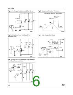
SWITCHING ON
Symbol
Parameter
Test Conditions
Min.
Typ.
Max.
Unit
t
V
R
= 100V, I =16 A
Turn-on Delay Time
25
ns
d(on)
DD
D
= 4.7Ω, V = 10V
G
GS
t
Rise Time
50
ns
r
(see test circuit, Figure 3)
Q
V
V
= 160V, I = 33 A,
D
Total Gate Charge
Gate-Source Charge
Gate-Drain Charge
117
15
158
nC
nC
nC
g
DD
= 10V, R = 4.7Ω
GS
G
Q
gs
Q
50
gd
SWITCHING OFF
Symbol
Parameter
Off-voltage Rise Time
Fall Time
Test Conditions
Min.
Typ.
60
Max.
Unit
ns
t
V
R
= 160V, I = 16 A,
r(Voff)
DD
D
= 4.7Ω, V = 10V
G
GS
t
40
ns
f
(see test circuit, Figure 5)
t
Cross-over Time
100
ns
c
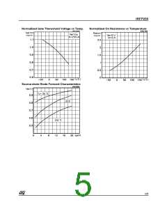
SOURCE DRAIN DIODE
Symbol
Parameter
Test Conditions
Min.
Typ.
Max.
33
Unit
A
I
Source-drain Current
SD
I
(2)
(1)
Source-drain Current (pulsed)
Forward On Voltage
132
1.6
A
SDM
V
I
I
= 33 A, V = 0
V
SD
SD
GS
t
= 33 A, di/dt = 100A/µs,
Reverse Recovery Time
Reverse Recovery Charge
Reverse Recovery Current
370
5.4
29
ns
µC
A
rr
SD
V
= 100V, T = 150°C
j
DD
Q
rr
(see test circuit, Figure 5)
I
RRM
Note: 1. Pulsed: Pulse duration = 300 µs, duty cycle 1.5 %.
2. Pulse width limited by safe operating area.
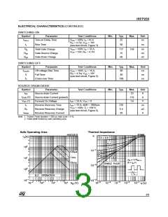
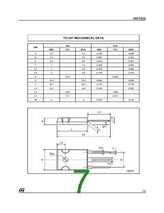
Safe Operating Area
Thermal Impedance
3/8

 STMICROELECTRONICS [ ST ]