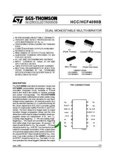
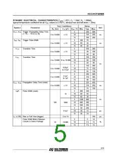
HCC/HCF4098B
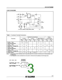
pulse one period) on the application of each new
trigger pulse. For operation in the non-triggerable
mode, Q is connected to –TR when leading-edge
triggering (+ TR) is used or Q is connected to + TR
when trailing-edge triggering (– TR)isused. Thetime
period (T) for this multivibrator can be approximated
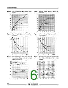
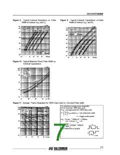
by TX = 1/2 RX CX for CX ≥ 0.01 µF. Time periods as
a function of RX forvalues of CX and VDD are given in
fig. 8. Values of T vary from unit to unit and as a func-
tionofvoltage, temperature, andRX CX. The minimum
value of external resistance, RX, is 5 kΩ. The maxi-
mum value of external capacitance, CX, is 100µF.
Fig.9showstimeperiods asafunctionof CX forvalues
of RX and VDD. The output pulse width has vari-
ations of ±2.5 % typically, over the temperature range
of – 55°C to 125° C for CX = 1000pF and RX = 100
kΩ. For power supply variations of ± 5%, the output
pulse width has variations of ± 0.5% typically, for VDD
= 10V and 15V and ± 1% typically, for VDD = 5 V at
CX = 1000 pF and RX = 5kΩ.
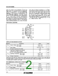
FUNCTIONAL DIAGRAM
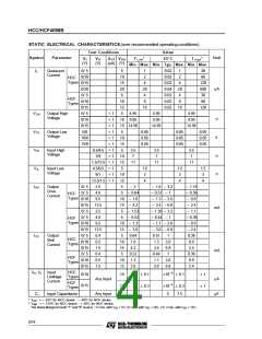
ABSOLUTE MAXIMUM RATINGS
Symbol
Parameter
Supply Voltage : HCC Types
HCF Types
Value
Unit
VDD
*
– 0.5 to + 20
– 0.5 to + 18
V
V
Vi
II
Input Voltage
– 0.5 to VDD + 0.5
V
DC Input Current (any one input)
± 10
mA
mW
Pto t
Total Power Dissipation (per package)
Dissipation per Output Transistor
200
for To p = Full Package-temperature Range
100
mW
Top
Operating Temperature : HCC Types
HCF Types
– 55 to + 125
– 40 to + 85
°C
°C
Tstg
Storage Temperature
– 65 to + 150
°C
Stresses above those listed under ”Absolute Maximum Ratings” may cause permanent damage to the device. This is a stress rating only
and functional operation of the device at these or any other conditions above those indicated in the operational sections of this specification
is not implied. Exposure to absolute maximum rating conditions for external periods may affect device reliability.
* All voltage values are referred to VSS pin voltage.
RECOMMENDED OPERATING CONDITIONS
Symbol
Parameter
Supply Voltage : HCC Types
HCF Types
Value
Unit
VDD
3 to 18
3 to 15
V
V
VI
Input Voltage
0 to VDD
V
To p
Operating Temperature : HCC Types
HCF Types
– 55 to + 125
– 40 to + 85
°C
°C
2/14

 STMICROELECTRONICS [ ST ]