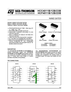
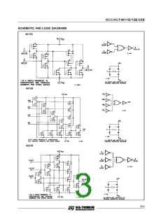
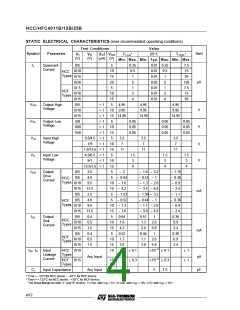
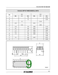
HCC/HFC4011B/12B/23B
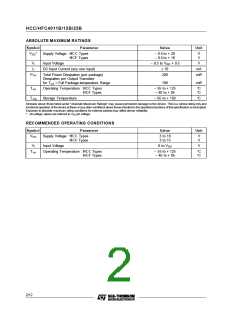
ABSOLUTE MAXIMUM RATINGS
Symbol
Parameter
Value
Unit
VDD
*
Supply Voltage : HCC Types
HCF Types
– 0.5 to + 20
– 0.5 to + 18
V
V
Vi
II
Input Voltage
– 0.5 to VDD + 0.5
V
DC Input Current (any one input)
± 10
mA
mW
Pto t
Total Power Dissipation (per package)
Dissipation per Output Transistor
200
for To p = Full Package-temperature Range
100
mW
Top
Operating Temperature : HCC Types
HCF Types
– 55 to + 125
– 40 to + 85
°C
°C
Tstg
Storage Temperature
– 65 to + 150
°C
Stresses above those listed under ”Absolute Maximum Ratings” may cause permanent damage to the device. This is a stress rating only and
functional operation of thedevice atthese orany other conditions above thoseindicatedin the operationalsections of this specification is notimplied.
Exposure to absolute maximum rating conditions for external periods may affect device reliability.
*
All voltage values are referred to VSS pin voltage.
RECOMMENDED OPERATING CONDITIONS
Symbol
Parameter
Supply Voltage : HCC Types
HCF Types
Value
Unit
VDD
3 to 18
3 to 15
V
V
VI
Input Voltage
0 to VDD
V
Top
Operating Temperature : HCC Types
HCF Types
– 55 to + 125
– 40 to + 85
°C
°C
2/12

 STMICROELECTRONICS [ ST ]